Connect with us

Technology

AI Impact on Electron Microscope Market growth, set to increase by USD 1.72 billion from 2024-2028, Rising need for root-cause failure analysis to boost the revenue, Technavio

Published

on

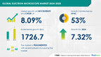
NEW YORK, Aug. 22, 2024 /PRNewswire/ — The global electron microscope market  size is estimated to grow by USD 1.72 billion from 2024-2028, according to Technavio. The market is estimated to grow at a CAGR of about 8.09%  during the forecast period.  Rising need for root-cause failure analysis is driving market growth, with a trend towards increased demand for lvems. However, high product cost and heavy excise duties  poses a challenge. Key market players include Advantest Corp., Agilent Technologies Inc., Bruker Corp., Carl Zeiss AG, COXEM Co. Ltd., Danaher Corp., DELONG INSTRUMENTS AS, Hirox Co. Ltd., HOVERLABS, JEOL Ltd., Keysight Technologies Inc., Nikon Corp., Nion, Novartis AG, Olympus Corp., Seiko Holdings Corp., TESCAN GROUP, Thermo Fisher Scientific Inc., Topcon Corp., and UNISOKU Co. Ltd..

Get a detailed analysis on regions, market segments, customer landscape, and companies – Click for the snapshot of this report

Forecast period

2024-2028

Base Year

2023

Historic Data

2018 – 2022

Segment Covered

Application (Semiconductors, Life sciences, Material sciences, and Nanotechnology), Technology (SEM, TEM, and DBEM), End-user (Industries, Institutions, and Others), and Geography (APAC, North America, Europe, Middle East and Africa, and South America)

Region Covered

APAC, North America, Europe, Middle East and Africa, and South America

Key companies profiled

Advantest Corp., Agilent Technologies Inc., Bruker Corp., Carl Zeiss AG, COXEM Co. Ltd., Danaher Corp., DELONG INSTRUMENTS AS, Hirox Co. Ltd., HOVERLABS, JEOL Ltd., Keysight Technologies Inc., Nikon Corp., Nion, Novartis AG, Olympus Corp., Seiko Holdings Corp., TESCAN GROUP, Thermo Fisher Scientific Inc., Topcon Corp., and UNISOKU Co. Ltd.

Key Market Trends Fueling Growth

The electron microscope market is witnessing significant growth due to the increasing demand for low-voltage electron microscopes (LVEMs), particularly in life sciences, material science, pathology, and nanomaterials applications. LVEMs operate at a lower voltage (less than 25kV) than high-voltage electron microscopes (HVEMs), making them suitable for installation in any lab. Their advantages include being compact, cost-effective, and causing minimal damage to specimens, especially those with a low atomic number. LVEMs, such as Delong America’s LVEM5 and LVEM25, offer multiple modes and can function as a TEM, SEM, STEM, or DBEM. Although LVEMs have lower magnification capabilities compared to HVEMs, their affordability and versatility make them an essential addition to research facilities. Technavio anticipates the global electron microscope market to continue expanding due to the rising demand for these innovative microscopes. 

The Electron Microscope market is thriving with trends like digital microscopy and high-resolution imaging. Improvements in image resolution help eliminate distorted images, ensuring better quality control. Open-source software and closed-source software are popular choices for skilled professionals in various industries. Neuronstudio and L-measure are leading software solutions. Physicists and laboratory technicians in sectors like surface physics, surface analyses, and nanotechnology research use these microscopes for magnification, depth of field, and topographical, morphological, compositional information. Industries like gemology, metallurgy, pharmaceutical and biotechnology, semiconductor and electronics, textiles, natural resources, aeronautics, automotive, apparel, pharmaceutical, industrial failure analysis, process control, and life science rely on Electron Microscopes for their specific needs. Super-resolution microscopy, artificial intelligence-based imaging, and correlative microscopy are the latest advancements. Trade regulations ensure safety and ethical use. Electron Microscopes are essential scientific instruments for disease diagnostics, biological sciences, healthcare facilities, and alternative imaging technologies. 

Discover a Comprehensive 360° Market Analysis: Understand the Impact of AI. For detailed information- Request Sample!

Market Challenges

The electron microscope market involves significant upfront costs, making sales to research institutions heavily reliant on government and corporate funding. This funding, however, is subject to change and can create market uncertainty. Additionally, import duties and taxes, such as customs duties, levied by various governments on electron microscopes add to the final product price. These taxes serve as revenue generation strategies for governments. In some countries, the same government that funds research institutions imposes these taxes. The taxation can take the form of direct or indirect taxes, with rates varying from 11% in the US to 17% in Brazil. An increase in taxes and duties raises the overall cost of electron microscopes, potentially hindering market growth during the forecast period.The Electron Microscope Market is experiencing significant growth, particularly in the Lifesciences segment. Scanning electron microscopes (SEMs) are driving innovation, with educational institutions and nanotech research leading the way. Funding for nanotechnology, semiconductors, material sciences, and life sciences is increasing, fueling the development of new nanomaterials and nanotechnology-based devices. Challenges include the need for high resolution power, advanced features like surface topography analysis, and the involvement of quality control personnel. The semiconductor industry relies on electron microscopes for failure analysis, detection, and lithography. Nanotechnology applications include imaging at the atomic scale, and the development of new microscopes like cryo-electron microscopy, digitization, and live-cell imaging. Rising technological advancements are leading to super resolution, high throughput methods, expansion microscopes, scanning helium microscopes, and multi-view microscopes. Clinical trials, pathology, diagnosis of diseases like toxicology and forensics, immune electron microscopy, and cryo-electron microscopy are all benefiting from these advancements. The market is expected to continue expanding as new applications and integrated microscopy workflows emerge.

For more insights on driver and challenges – Download a Sample Report

Segment Overview 

This electron microscope market report extensively covers market segmentation by

Application 1.1 Semiconductors1.2 Life sciences1.3 Material sciences1.4 NanotechnologyTechnology 2.1 SEM2.2 TEM2.3 DBEMEnd-user 3.1 Industries3.2 Institutions3.3 OthersGeography 4.1 APAC4.2 North America4.3 Europe4.4 Middle East and Africa4.5 South America

1.1 Semiconductors-  The Electron Microscope Market has experienced steady growth due to increasing demand from various industries such as semiconductor, materials science, and biotechnology. These microscopes provide high-resolution images, enabling advancements in research and development. Key players include FEI Company, JEOL Ltd., and Carl Zeiss AG, who invest in innovation and expansion to meet market needs. The market’s future looks promising with ongoing technological advancements and growing applications.

For more information on market segmentation with geographical analysis including forecast (2024-2028) and historic data (2018 – 2022)  – Download a Sample Report

Research Analysis

The Electron Microscope Market is experiencing significant growth, particularly in the Lifesciences segment, driven by the increasing demand for high-resolution imaging in research and development. Scanning electron microscopes (SEMs) are a popular choice due to their ability to provide detailed images of various surfaces, including skinny wafers in the semiconductor industry and nanotech research. Product innovation is a key factor in the market’s expansion, with new technologies such as expansion microscopes, scanning helium microscopes, and multi-view microscopes gaining popularity. High throughput methods and integrated microscopy workflows are also driving efficiency and productivity in the market. Digital microscopy and image resolution continue to be important areas of focus, with advancements in technology helping to minimize distorted images. Import-Export Analysis reveals that the market is global in nature, with key application niches including biologics and transmission electron microscopes. The integration of Artificial Intelligence (AI) and Machine Learning (ML) is also transforming the market, enabling faster and more accurate image analysis.

Market Research Overview

The Electron Microscope Market is witnessing significant growth due to the rising technological advancement in various industries, particularly in the lifesciences segment. Scanning electron microscopes (SEMs) are gaining popularity for their ability to provide high-resolution images of surface topography and morphological, compositional information at the atomic scale. Nanotech research, semiconductors, material sciences, and nanomaterials are some key areas driving the market’s growth. Product innovation is a major trend, with new features such as digitization, live-cell imaging, super resolution, high throughput methods, expansion microscopes, scanning helium microscopes, multi-view microscopes, and integrated microscopy workflows. Educational institutions are also investing in electron microscopes for research and teaching purposes. Funding for nanotechnology-based research and development is another growth driver, particularly in the areas of nanotechnology, lithography, coating, failure analysis, detection, semiconductor devices, and nanotechnology-based devices. The market caters to various industries, including lifesciences, pharmaceutical and biotechnology, semiconductor and electronics, textiles, natural resources industries, aeronautics, automotive, apparel, and industrial failure analysis. Quality control personnel in these industries rely on electron microscopes for surface physics and surface analyses, magnification, depth of field, and high-resolution imaging. The market also offers open-source and closed-source software solutions such as Neuronstudio and L-measure, which are preferred by skilled professionals, including physicists and laboratory technicians. The market’s growth is further fueled by the increasing demand for atomic force scanning, cryo-electron microscopy, and correlative microscopy in fields such as gemology, metallurgy, and forensics. Clinical trials, pathology, diagnosis of diseases, toxicology, and immune electron microscopy are some other applications driving the market’s growth. Despite the market’s potential, challenges such as distorted images, quality control, and the high cost of electron microscopes and associated equipment remain. However, ongoing research and development efforts are addressing these challenges, ensuring the market’s continued growth.

Table of Contents:

1 Executive Summary
2 Market Landscape
3 Market Sizing
4 Historic Market Size
5 Five Forces Analysis
6 Market Segmentation

ApplicationSemiconductorsLife SciencesMaterial SciencesNanotechnologyTechnologySEMTEMDBEMEnd-userIndustriesInstitutionsOthersGeographyAPACNorth AmericaEuropeMiddle East And AfricaSouth America

7 Customer Landscape
8 Geographic Landscape
9 Drivers, Challenges, and Trends
10 Company Landscape
11 Company Analysis
12 Appendix

About Technavio

Technavio is a leading global technology research and advisory company. Their research and analysis focuses on emerging market trends and provides actionable insights to help businesses identify market opportunities and develop effective strategies to optimize their market positions.

With over 500 specialized analysts, Technavio’s report library consists of more than 17,000 reports and counting, covering 800 technologies, spanning across 50 countries. Their client base consists of enterprises of all sizes, including more than 100 Fortune 500 companies. This growing client base relies on Technavio’s comprehensive coverage, extensive research, and actionable market insights to identify opportunities in existing and potential markets and assess their competitive positions within changing market scenarios.

Contacts

Technavio Research
Jesse Maida
Media & Marketing Executive
US: +1 844 364 1100
UK: +44 203 893 3200
Email: media@technavio.com
Website: www.technavio.com/

View original content to download multimedia:https://www.prnewswire.com/news-releases/ai-impact-on-electron-microscope-market-growth-set-to-increase-by-usd-1-72-billion-from-2024-2028–rising-need-for-root-cause-failure-analysis-to-boost-the-revenue-technavio-302228627.html

SOURCE Technavio

Continue Reading

Technology

Axon Announces Body 5: Next-Generation Camera Built for the AI Era

Published

on

By

Axon Body 5 delivers 25x the AI processing power of earlier-generation cameras, with upgraded connectivity, audio and battery life to support real-time situational awareness in the field

SCOTTSDALE, Ariz., Oct. 24, 2026 /PRNewswire/ — Axon (Nasdaq: AXON), the global leader in public safety technology, today announced Axon Body 5, its newest body-worn camera designed to bring more powerful intelligence, connectivity and real-time support directly to officers in the field.

For years, Axon body cameras have helped agencies capture critical evidence and create greater transparency. Body 5 is built to help officers during the call, with information, assistance and backup on the spot.

“Officers shouldn’t have to choose between getting information and watching the scene. With Axon Body 5, they don’t,” said Rick Smith, Axon Founder and CEO. “They capture a license or document with the camera, keep their hands free and eyes up, and get information faster than writing it down and calling it in by radio. An officer fully engaged with the person in front of them, not down at a notepad, is a safer officer and a better-served community.”

Axon Body 5: Built for the AI Era

Built from the ground up for the AI era, Axon Body 5 delivers 25x the AI processing power than earlier generation Axon body cameras, alongside advancements in connectivity, audio, video and battery life. Together, these upgrades give the camera the physical power to run smarter AI features — both today and as new AI tools are developed in the future — while also making it more dependable for officers to use every day. 

For the first time, Axon is also introducing two versions of its latest flagship camera: Axon Body 5 and Axon Body 5 Pro.

Both models feature several key advancements, including:

25x more processing power for AI: A powerful new computing architecture creates the capacity to support current and future AI features directly on the body camera.Enhanced video: Improved video captures clearer evidence across challenging environments, including better low-light performance.Improved connectivity: Seamless connectivity in urban and remote environments – and more precise location capability – helps officers, cameras and remote support teams stay connected when timely information matters most.Longer battery life: 20% more battery life than the previous generation helps keep the camera ready and connected throughout an officer’s shift.

The Axon Body 5 Pro will continue to gain new AI capabilities as they become available, growing along with the AI Era Plan. Additionally, new hardware features include:

A near-focus camera: An additional dedicated camera lens lets officers scan driver’s licenses to check status and search for wants or warrants in seconds, without returning to the patrol vehicle, with relevant information sent to Axon Fusus to support real-time operations.Front-facing speakers: Four additional speakers project even more powerful audio toward the person an officer is speaking with, helping real-time translations from Axon Assistant carry more clearly over heavy traffic or crowd noise. Additional memory: Extra space lets the camera run several AI tools at once, helping officers stay better informed and work faster.

Bringing More of Axon’s AI Era Into the Field

Axon Body 5 helps officers get more out of the Axon AI Era Plan by bringing smart tools right to the scene. Axon’s portfolio already supports public safety professionals across a growing range of tasks. For example, Draft One helps officers turn body-camera audio into high-quality report drafts and Axon Assistant provides voice-based information access and real-time translation.

Increasingly, Axon is also bringing AI into real-time operations.

Axon Guardian is a new category of AI features within the AI Era Plan that was specifically created to work with an officer’s field-based devices – starting with body cameras and in-car cameras – to improve safety. Guardian is designed to flag potential risks as situations unfold and create alerts when additional attention may be needed. Two of the first features include:

Escalation Detection: When an Axon Body 4 or Axon Body 5 camera is activated and recording, Guardian has the ability to detect potential conflicts in real time and create an alert in Axon Fusus. A human reviews the livestream and decides if additional support or action is needed.Approach Alert: When active on Axon Fleet 3, Guardian can detect if the door of a stopped vehicle opens and alert the officer through the in-car display and their body-worn camera.

Combined, Axon Body 5 and the expanding AI Era portfolio demonstrate the importance of AI as a critical resource to assist public safety professionals before, during and after an incident — reducing administrative burden, improving situational awareness and helping protect more lives.

Innovating Responsibly

Axon’s Responsible Innovation framework guides the development of all of its products. Designed with this in mind, Axon Body 5 and Guardian prioritize human oversight and maintain agency control over data. As a key part of the responsible innovation process, Axon’s independent Ethics and Equity Advisory Council was created to help responsibly develop and deploy new technologies with transparency, while aligning with community expectations.

General availability dates for Axon Body 5 and Axon Guardian will be announced soon. Product features and capabilities vary by configuration. For more information on Axon’s current products and services: Axon Product Catalog – Axon.com.

About Axon
Axon (Nasdaq: AXON) is the global leader in public safety technology supporting state, local, federal and international public safety agencies with technology designed to Protect Life. Complementing its mission, Axon’s growing Enterprise market focuses on protecting critical infrastructure and frontline workers across multiple industries including corporate security, hospitality, retail and healthcare. Founder-led since 1993, Axon builds products with transparency and responsibility. From TASER energy devices to today’s connected network of hardware – including cameras, drones, and robotics – cloud software, sensors, and AI-tools, the Axon ecosystem helps seamlessly protect people and places when it matters most. To ensure these technologies align with community expectations, Axon’s independent Ethics & Equity Advisory Council guides the ethical, inclusive, and accountable design of its products and services. Learn more about the EEAC and Axon’s Responsible Innovation framework at Axon Responsibility. 

Non-Axon trademarks are the property of their respective owners. Axon, TASER and the Delta Logo are trademarks of Axon Enterprise, Inc., some of which are registered in the US and other countries. For more information, visit www.axon.com/legal. All rights reserved.

Please visit https://investor.axon.com and https://www.axon.com/newsroom for more information.

Media Contact:
Kate MacKinnon
Vice President, Communications
press@axon.com

View original content to download multimedia:https://www.prnewswire.com/news-releases/axon-announces-body-5-next-generation-camera-built-for-the-ai-era-302918553.html

SOURCE Axon

Continue Reading

Technology

In HelloNation, Custom Fabrication Expert Mark Coyle Explains a Common Mistake in Custom Aluminum Design

Published

on

By

The article explains why smart geometry, not thicker walls, creates stronger, more efficient aluminum components.

ROCHESTER, N.Y., Oct. 24, 2026 /PRNewswire/ — What early design choice causes many custom aluminum projects to become heavier, costlier, or harder to manufacture? That question is addressed in a HelloNation article featuring insights from Custom Fabrication Expert Mark Coyle of American Custom Metals, Inc. in Rochester, New York, that outlines how misunderstanding aluminum behavior leads designers to rely on thick walls instead of stronger geometry.

The article begins by explaining that many people assume thicker walls automatically make aluminum parts stronger. It notes that aluminum does not respond to wall thickness the way steel does. Instead, its performance is shaped by how the metal flows through the extrusion die. The article states that custom aluminum design is more effective when profiles use ribs, chambers, and flanges to create stiffness without adding unnecessary weight. This guidance helps readers understand why adding material often increases cost without improving strength.

The article also highlights that thicker walls change how aluminum moves during extrusion. When heavy areas fill more slowly, the metal cools unevenly and can develop stress that only appears later. The HelloNation piece explains that well-balanced geometry keeps extrusion smooth and predictable. This consistency makes it easier to maintain dimensional accuracy across long production runs. By focusing on geometry, custom aluminum design avoids the problems that come with slow extrusion speeds and uneven cooling.

Another insight in the article centers on how ribs and internal supports influence stability. It describes how a thin wall supported by a properly placed rib often performs better than a thick wall with no reinforcement. This happens because the rib helps distribute load, improve stiffness, and guide the aluminum as it cools. The article explains that this structural approach makes custom aluminum design more efficient and gives designers more control over how the final part behaves under pressure.

The article also shows why early collaboration between designer and fabricator prevents costly changes. It states that a fabricator familiar with extrusion can catch potential issues before a die is built. Small adjustments to corners or transitions can remove weak points or improve metal flow. The article notes that this teamwork keeps the design aligned with real-world production. By working together early, both sides reduce the risk of redesigning the die after the first test run.

Machining is another area where the article explains how wall thickness affects performance. Features such as deep pockets or sharp internal angles may require slow feed rates or special tooling. When walls are thicker than needed, those areas can become difficult to machine cleanly. The article states that thoughtful custom aluminum design makes machining more predictable. Small changes, such as adding radiused edges or sizing features to match standard tools, help shorten cycle times and prevent tool wear.

Thermal behavior receives detailed attention as well. The article explains that aluminum retains heat differently depending on the mass of each section. Thicker walls hold heat longer, which increases the chance of distortion during extrusion, machining, or finishing. When a design uses geometry to create strength, the material cools more evenly. This reduces warping and helps long profiles stay aligned. The article notes that stable cooling is important for components that require a precise fit and consistent shape throughout an entire production run.

Cost is also a key topic in the article. It states that heavier profiles increase material use, extrusion time, and tooling needs. A custom aluminum design that relies on geometry instead of mass lowers material consumption and keeps the fabrication process efficient. The article explains that lighter parts are easier to handle, ship, and assemble. This saves money across multiple stages of production and supports long-term manufacturing efficiency.

The article also notes that smart custom aluminum design creates profiles that behave predictably during extrusion and machining. Smooth transitions, balanced wall dimensions, and structural features help reduce the chance of distortion or dimensional drift. These elements also lower scrap rates and support reliable performance. By using geometry instead of excess material, designers build parts that maintain strength without compromising manufacturability.

As the article concludes, it emphasizes that avoiding thick walls is one of the best ways to improve performance and lower cost. It states that the most dependable custom aluminum components come from designs that use structural features to strengthen the profile. When designers understand how aluminum behaves at each stage of extrusion and machining, they create parts that are strong, efficient, and consistent from batch to batch. This approach turns custom aluminum design into a predictable process rather than a series of uncertain adjustments.

A Common Mistake in Custom Aluminum Design features insights from Mark Coyle, Custom Fabrication Expert of Rochester, NY, in HelloNation.

About HelloNation
HelloNation is America’s Good News Network, a premier media platform built on the idea that good news travels faster when real people tell real stories. Through its community-focused publications and innovative “edvertising” approach, HelloNation delivers content that informs, inspires, and spotlights the leaders making a meaningful impact in their communities.

View original content to download multimedia:https://www.prnewswire.com/news-releases/in-hellonation-custom-fabrication-expert-mark-coyle-explains-a-common-mistake-in-custom-aluminum-design-302918282.html

SOURCE HelloNation

Continue Reading

Technology

World Young Scientist Summit 2026 Opens in Wenzhou, Zhejiang

Published

on

By

WENZHOU, China, Oct. 24, 2026 /PRNewswire/ — This is a report by China Daily:

On October 24, the World Young Scientist Summit 2026 opened in Wenzhou, Zhejiang. The event is hosted by the China Association for Science and Technology (CAST), the Zhejiang Provincial People’s Government, and the World Association of Young Scientists. Nearly 800 representatives, including scientists, educators, and entrepreneurs from more than 60 countries and regions, are attending the summit.

He Junke, Vice President of CAST in charge of daily work and First Secretary of its Secretariat; Lian Yimin, Chairman and Party Group Secretary of the Zhejiang Provincial Committee of the Chinese People’s Political Consultative Conference; Marcelo Knobel, Executive Director of The World Academy of Sciences; and Zhang Zhenfeng, Member of the Standing Committee of the CPC Zhejiang Provincial Committee and Secretary of the CPC Wenzhou Municipal Committee, attended the summit and delivered remarks. Yao Gaoyuan, Vice Governor of the Zhejiang Provincial People’s Government, presided over the first segment of the plenary session.

With the theme “Gathering Talents Worldwide to Create a Better Future,” the summit’s annual agenda is “Global Youth Action in the AI Era: Building a Sustainable Future.” It aims to draw on the insights of young people around the world, deepen international sci-tech cooperation, and jointly address questions about young people, science, the world and the future.

Efim Zelmanov, Fields Medalist and Foreign Member of the Chinese Academy of Sciences; Chen Yunji, Deputy Director of the Institute of Computing Technology, CAS, and Director of the National Key Laboratory of Processor Chips; Mary Garson, President of the International Union of Pure and Applied Chemistry; and Lu Chaoyang, Member of the Standing Committee of CAST, Executive Dean of the Shanghai Institute of Advanced Study, University of Science and Technology of China, and Chairman of the Council of the World Association of Young Scientists, delivered keynote speeches respectively on education reform in the AI era, AI and processor chips, young women scientists’ participation in science, and quantum computing. They explored new opportunities for scientific research, talent cultivation, and international cooperation in the AI era.

This year’s summit placed greater emphasis on the growth needs of young scientists, with young talents under the age of 45 accounting for 88 percent of participants. It aimed to build a cluster of international journals, bring together young scientific talent, facilitate a batch of international collaborative projects and advance the application and commercialization of scientific and technological achievements. The summit released the Report on the Distribution and Mobility of Young Scientists in the Field of Embodied Intelligence, launched the World Young Scientist Summit Partner Journal Program and the 2026 World Young Scientist Innovation and Entrepreneurship Growth Support Program. It also published the “Young Scientist Pioneers 2035” list and announced the 2026 Sustainable Development Young Scientist Award. The awards were presented to four Chinese and foreign scientists.

Chen Tianrun, Founder of Hangzhou Moxin Technology Co., Ltd.; Yuan Yang, Assistant to the Dean of the Institute for Interdisciplinary Information Sciences at Tsinghua University; and two of the 2026 Sustainable Development Young Scientist Award winners, César de la Fuente and Nicola Segata, among other Chinese and foreign young scientist representatives, spoke at the flash-talk session to share their research practices and reflections.

In addition, the conference focused on fields such as future manufacturing, quantum information, embodied intelligence, brain-computer intelligence, environmental science, deep-sea resources, and life and health, and held 12 parallel forums. It also included the “Gravitation π” Future Technology and Concept Products Exhibition and Exchange, local thematic side events, and sci-tech and humanities study visits, further building an interdisciplinary, cross-regional and cross-sector platform for youth sci-tech exchange and cooperation.

View original content to download multimedia:https://www.prnewswire.com/news-releases/world-young-scientist-summit-2026-opens-in-wenzhou-zhejiang-302918664.html

SOURCE China Daily

Continue Reading

Trending