Connect with us

Technology

Sony Semiconductor Solutions to Release X-ray CMOS Sensor with Industry’s Fastest(*1) Imaging and Low-Noise Performance for Inspection and Measurement Instrumentation

Published

on

High-accuracy energy measurements and photon-level data acquisition on a single chip

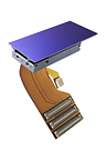
ATSUGI, Japan, June 8, 2026 /PRNewswire/ — Sony Semiconductor Solutions Corporation (Sony) today announced the upcoming release, mass-production, and shipment of the IMX711 direct conversion charge-integrating X-ray CMOS image sensor.

The IMX711 is an X-ray image sensor for inspection and measurement instrumentation which directly detects X-rays and outputs signals proportional to their energy. The new sensor offers the industry’s fastest*1 maximum 26,100 fps high-speed imaging, achieved thanks to Sony’s proprietary circuit technology, suppressing charge saturation for accurate measurements. It also significantly reduces noise to enable improved signal detection precision in low-flux conditions, detecting differences in photon energy. It provides both high-accuracy measurements of integrated X-ray energy at a wide dynamic range and energy information acquisition at the photon level on a single sensor, a feat that has been difficult with conventional sensors. This unique feature will contribute to the advancement and diversification of X-ray inspection and measurement technologies, which are used in a wide variety of applications, from cutting-edge device inspection to scientific measurements.

*1     Among charge-integrating X-ray CMOS image sensors. According to Sony research (as of announcement on June 9, 2026)

.


Model name

Mass-production shipment date

IMX711 3.73-type (27.88 mm × 52.85 mm HW), 
approximately 280,000 effective pixel*2 direct conversion charge-
integrating X-ray CMOS image sensor

First quarter of FY2026

*2    Based on the image sensor effective pixel specification method.

The IMX711 was developed with the collaboration between Sony Semiconductor Solutions Corporation and RIKEN. Based on a pixel structure invented by Dr. Takaki Hatsui of RIKEN, the two parties worked together on the technological development required to make it viable as a practical X-ray image sensor, including improving sensitivity and achieving high resistance to X-ray irradiation and high-voltage tolerance. Sony developed its circuit technology, manufacturing processes and packaging technology for mass production.

X-ray inspection and measurement are widely used in a variety of fields, including inspection of advanced devices such as batteries and semiconductors, and scientific measurement in materials development and life sciences research. As these methods become more sophisticated along with advances in data analysis technology including AI, X-ray sensors are also required to evolve to deliver more efficient and highly reliable data acquisition. However, with conventional sensors,*3 it has been challenging to improve measurement accuracy and meet the requirements of diversifying downstream analysis, due to the photon counting errors in high-flux conditions and the impact of noise under low-flux conditions.

The new sensor enables the industry’s fastest*1 maximum frame rate of 26,100 fps and low-noise performance of 34 e-rms*4 (random noise of approximately 34 electrons per pixel), thereby helping to resolve the above-mentioned technical challenges. It not only accurately detects signals across a wider dynamic range than conventional sensors, but also resolves photons of varying energy levels at high resolution while offering the advantage of a charge-integrating sensor to output both integrated X-ray energy data and photon energy data. The highly reliable data acquired by this product will not only improve the performance of X-ray inspection and measurement equipment, but also contribute to the development of new analysis methods using energy information, as described below.

*3    There are two types of conventional X-ray sensors: photon-counting and charge-integrating. With photon-counting sensors that process the X-ray signal based on thresholds, the measurement precision is high under low-flux conditions, but some photons may not be counted correctly as the signal becomes stronger. On the other hand, charge-integrating sensors output photon energy as a signal with integrated energy, but the impact of noise results in reduced measurement precision under low-flux conditions.
 

*4    An evaluation result. This result is calculated based on the average value of pixels in the sensor’s effective area in an environment where the sensor’s internal operating temperature is at or below 20 ℃. The functional guaranteed value is 60 e-rms.

Examples of Potential Applications

Improving precision and throughput in high-speed inspection of moving objects for battery and semiconductor applicationsElemental mapping for distinguishing photons of different energy levels and rendering two-dimensional distributionSimultaneous measurement of crystal structure analysis and element analysis using photon energy information and spatial information

Main Features

High-accuracy measurements in a wide dynamic range thanks to the industry’s fastest,*1 low-noise imaging
This product achieves the industry’s fastest*1 maximum frame rate of 26,100 fps thanks to Sony’s proprietary circuit technology. Lowering the amount of accumulated charge per frame enables superior saturation characteristics compared to conventional sensors. At the same time, random noise, which is a technical challenge on charge-integrating sensors, has been reduced to 34 e-rms*4 so that even faint X-ray signals are not obscured by noise and can be reliably detected. This improves measurement precision under low-flux conditions, offering photon level detection. These features enable accurate measurement of integrated X-ray energy for all pixels across low- to high-flux conditions, supporting inspection and measurement with significant differences in brightness on a single sensor, contributing to improved device throughput and an expanded dynamic range.High energy resolution enabling inspection and measurement using photon energy
The new sensor uses the charge-integrating method, which makes it possible to acquire photon energy information without the need to set a threshold in advance. Furthermore, noise and signal variation are suppressed during reading to achieve high energy resolution for clear identification of differences in photon energy. Enabling acquisition of highly reliable data via high energy resolution will contribute to streamlining and improving precision in advanced inspection and measurement, which previously required several measurements in applications such as detecting differences in constituent elements at the element level and structural and material analysis to quantitatively evaluate minute state changes. It also enables post-processing under various conditions such as collecting the measurement data for all pixels, combining it with spatial information, and extracting specific energy data contributes to multifunctional inspection and measurement.

Related Link
IMX711 product page: https://www.sony-semicon.com/en/products/is/scientific/x-ray.html

Key Specifications

Model name

IMX711-AABY

Image size

Diagonal 59.8 mm (Type 3.73)
27.88 mm (H) × 52.85 mm (V)

Number of active pixels

384 (H) × 728 (V) – 16*5
Approx. 0.28 megapixels

Unit cell size

72.6 μm (H) × 72.6 μm (V)

Substrate material

Silicon

Sensor thickness

650 μm

Frame rate
(All-pixel readout)

26.1 k fps (Mode-A)
17.4 k fps (Mode-C Cont, HDR)

Noise

Typ 34 e-rms*6
Max 60 e-rms

Saturation count rate (12keV)

0.94 Mcps/pixel (Mode-A)

33 Mcps/pixel (Mode-C Cont)

600 Mcps/pixel (Mode-C HDR)

Output interface

SLVS-EC

Package

Chip Size Package (CSP) : 30.36 mm (H) x 69.74 mm (V)

*5    Black pixels

*6    Typical value, averaged from measured values of active pixels at Tj = 20℃.

View original content to download multimedia:https://www.prnewswire.com/news-releases/sony-semiconductor-solutions-to-release-x-ray-cmos-sensor-with-industrys-fastest1-imaging-and-low-noise-performance-for-inspection-and-measurement-instrumentation-302793514.html

SOURCE Sony Electronics, Inc.

Continue Reading

Technology

Ascendion Expands AI Advisory Community with Four Global Business and Technology Leaders

Published

on

By

Former Global CTO of Banco Santander, former Group CIO of Currys, former CEO of IBPAP, and former Microsoft CVP and CTO of AI join the advisory community

Advisors will provide guidance on AAVA platform innovation, AI strategy, C-suite alignment, and enterprise adoption across Asia-Pacific, Europe, North America, and the UK

The growing community of advisors will bring practitioner perspective closer to Ascendion as enterprises move AI from experimentation to governed, production-scale outcomes

BASKING RIDGE, N.J., Oct. 27, 2026 /PRNewswire/ — Ascendion, an AI-native software engineering company, today announced the appointment of four global business and technology leaders to its AI Advisory Community: Andy Gamble, Jack Madrid, Julieta Ross, Ph.D., and Joseph Sirosh, Ph.D. 

The advisors bring perspectives rarely found in one group: executives who answered to Boards, regulators, and C-suites for what technology actually delivered; a builder of AI and data platforms at global scale; and a leader who shaped one of the world’s largest technology-services and talent ecosystems. Their experience spans banking, high-tech, media, and retail. Each will work directly with Ascendion’s regional and engineering leaders, so their counsel reaches the decisions it is meant to shape. 

“We are changing how software gets built. Enterprise leaders have moved past experiments. They want AI that delivers outcomes boards can measure and risk they can manage. Andy, Jack, Julieta, and Joseph have the experience and know where transformation succeeds. They will challenge our thinking, raise our ambition, and help us navigate a period of intense — and exciting — change,” said Karthik Krishnamurthy, CEO, Ascendion. 

Each advisor will map to a different part of the business, strengthening Ascendion’s alignment with leadership communities across the globe. 

Julieta Ross, Ph.D., former Global CTO of Banco Santander, brings two decades of leading technology inside global banks, along with public-company board experience. She will work with Ascendion’s leadership on executive relationships, go-to-market strategy, and growth, and will help the company meet the governance, regulatory, and risk expectations that banking and financial services leaders place on AI. Andy Gamble, former Group CIO of Currys plc, has spent nearly three decades as a technology buyer and transformation leader across consumer electronics, industrial, and retail businesses. He will advise Ascendion’s work across Europe and the UK, with a focus on consumer goods, manufacturing, and retail, and will share what executive teams and Boards expect from a technology partner. Joseph Sirosh, Ph.D., former Microsoft CVP and CTO of AI, has spent his career building and scaling machine learning platforms in the high-tech industry. He will advise Ascendion’s engineering leadership on the evolution of AAVA and its broader platform strategy as AAVA becomes an orchestration and harness layer for enterprise AI. Jack Madrid, former President and CEO of IBPAP, spent five years leading the industry association behind one of the world’s largest technology and business-services ecosystems, centered in the Philippines. He brings robust experience working across industries, including banking, high-tech, and media, and will advise Ascendion on Asia-Pacific markets and on how AI is reshaping global delivery, skills, and workforce models. 

Together, the advisors give Ascendion an outside perspective on the full spectrum of enterprise AI, from agentic platform strategy and product engineering to industry alignment and delivery. They will add capacity to Ascendion’s ongoing work on AI governance, helping ensure trusted impact from AI-native software engineering, and their practice-based insight will inform how Ascendion applies its Engineering to the Power of AI™ approach to commercial models, platform design, service execution, and workforce development. 

About Ascendion

Ascendion is a global AI-native software engineering company delivering trusted business outcomes – capital unlock, innovation velocity, lower risk – to 250+ enterprise clients. The company delivers business outcomes at scale by combining expert engineers, AI agents, and AAVA, Ascendion’s agentic AI platform. Together, they design, engineer, and operate production-ready software that improves everyday work and life. Learn more at www.ascendion.com.

Engineering to the Power of AI™, Engineering to Elevate Life™, and AAVA™ are trademarks or service marks of Ascendion. AAVA™ is pending registration. Unauthorized use is strictly prohibited.

View original content to download multimedia:https://www.prnewswire.co.uk/news-releases/ascendion-expands-ai-advisory-community-with-four-global-business-and-technology-leaders-302921368.html

Continue Reading

Technology

AvePoint Set to Join S&P SmallCap 600

Published

on

By

NEW YORK, Oct. 27, 2026 /PRNewswire/ — AvePoint Inc. (NASD: AVPT) will replace LXP Industrial Trust (NYSE: LXP) in the S&P SmallCap 600 effective prior to the opening of trading on Monday, November 2. Brookfield Asset Management Ltd. and Canada Pension Plan Investment Board are acquiring LXP Industrial Trust in a deal expected to close soon, pending final closing conditions.

Following is a summary of the changes that will take place prior to the open of trading on the effective date:

Effective Date

Index Name

Action

Company Name

Ticker

GICS Sector

Nov 2, 2026

S&P SmallCap 600

Addition

AvePoint

AVPT

Information Technology

Nov 2, 2026

S&P SmallCap 600

Deletion

LXP Industrial Trust

LXP

Real Estate

ABOUT S&P DOW JONES INDICES

S&P Dow Jones Indices is the largest global resource for essential index-based concepts, data and research, and home to iconic financial market indicators, such as the S&P 500® and the Dow Jones Industrial Average®. More assets are invested in products based on our indices than products based on indices from any other provider in the world. Since Charles Dow invented the first index in 1884, S&P DJI has been innovating and developing indices across the spectrum of asset classes helping to define the way investors measure and trade the markets.

S&P Dow Jones Indices is a division of S&P Global (NYSE: SPGI), which provides essential intelligence for individuals, companies, and governments to make decisions with confidence. For more information, visit www.spglobal.com/spdji/en/. 

FOR MORE INFORMATION:

S&P Dow Jones Indices
index_services@spglobal.com

Media Inquiries
spdji.comms@spglobal.com

View original content:https://www.prnewswire.com/news-releases/avepoint-set-to-join-sp-smallcap-600-302921327.html

SOURCE S&P Dow Jones Indices

Continue Reading

Technology

Archera Surpasses $5.6 Billion in Cloud and AI Spend Under Management, Closes Series C Led by Pivot Investment Partners, and Expands Insurance-Backed Cloud Commitments

Published

on

By

The round will help Archera expand its guaranteed cloud commitments, bringing insurance-backed financial protection to companies navigating unpredictable AI and cloud spending. The company has delivered more than $700 million in customer savings and now manages approximately $5.6 billion in annual cloud and AI spend.

BELLEVUE, Wash., Oct. 27, 2026 /PRNewswire/ — As artificial intelligence makes cloud spending harder to predict, companies face an increasingly expensive choice: commit to long-term cloud and AI contracts to unlock significant discounts or preserve flexibility and leave savings on the table. Archera has raised a $15 million Series C to expand its Guaranteed Commitments and change that equation.

The cloud economics company today announced it closed its Series C funding round, led by Pivot Investment Partners, with participation from existing investors including HighSage Ventures. The financing brings Archera’s total funding to $38.3 million. It will support the expansion of Archera’s Guaranteed Commitments and its suite of free cloud cost tools, including its FinOps Agent and MCP.

Insurance-backed financial protection is central to Archera’s next phase of growth. Archera purchased a policy on a surplus lines basis from Crum & Forster Specialty Insurance Company to back its guarantee. This model helps businesses pursue cloud commitment savings while managing the financial risk of usage changes.

The company has delivered more than $700 million in savings to over 2,200 organizations, including PubNub, Art.com, and Astronomer. The thesis behind Archera is simple: companies shouldn’t have to predict AI’s future to commit and save money on today’s infrastructure.

Why Cloud and AI Commitments Need to Change

Cloud providers reward customers who commit to spending over one- to three-year periods with substantial discounts and access to capacity. Historically, those commitments have helped businesses reduce infrastructure costs. But AI is changing the risk and economics of that decision.

A new model launch can multiply GPU spending in months. A more efficient model, a shift in architecture, or a move to a different service can reduce it just as quickly. Long-term commitments that once looked financially sound can become expensive liabilities.

Companies are left choosing between overcommitting and risking unused spend, or undercommitting and missing out on available discounts. Many choose the latter, sacrificing potential savings to preserve flexibility.

Archera believes that the trade-off is unnecessary. Its Guaranteed Commitments provide resource-level cloud and AI discounts with terms as short as 30 days. If usage declines and a covered commitment goes unused, Archera covers the cost under the terms of its guarantee.

The result is a different way to approach cloud purchasing. Businesses can pursue deeper discounts and unlock capacity otherwise gated behind a commitment, without bearing the entire financial consequence when actual usage diverges from forecasts.

Turning Cloud Optimization Into a Financial Product

Traditional cloud cost management tools provide visibility, recommendations, automation, and forecasting, but they can’t eliminate the financial risk of unused commitments. Archera combines its free FinOps platform and Agent with a financial guarantee that addresses inaccurate forecasts.

“Every tool in this market is trying to forecast your cloud usage a little better. We think that’s the wrong bet,” said Aran Khanna, co-founder and CEO of Archera. “Nobody can forecast AI demand, not the customer, not the cloud provider. So instead of predicting it, we guarantee it, and we have purchased an insurance policy to back that guarantee. If covered usage drops, we address the unused commitment cost under the terms of our guarantee. That’s a new way to purchase cloud, not another dashboard, and it’s why we’ve been able to return $700 million to our customers.”

The approach positions cloud commitments as a financial risk decision, helping finance and engineering leaders manage budgets while adapting to changing technology.

Built for CFOs, CTOs, and the Teams Managing AI Costs

The approach addresses a growing challenge across finance and engineering: how to control infrastructure costs without constraining the business.

For CFOs: Capture commitment-level discounts while reducing exposure to eligible unused spend under the guarantee.For CTOs and engineering leaders: Preserve flexibility to adopt new AI models, change architectures, and scale workloads without letting past commitments dictate future decisions.For FinOps teams: Increase commitment coverage with a financial backstop when usage changes, without more back-and-forth with engineering teams to get perfect forecasts.For cloud partners and resellers: Give customers a differentiated way to pursue cloud savings that can be reinvested in new cloud services while managing commitment risk.

Archera’s platform connects to AWS, Microsoft Azure, or Google Cloud billing data in read-only mode and analyzes actual usage. It then recommends and automates the purchasing of both native commitments and Archera Guaranteed Commitments.

Customers can evaluate their potential savings before making any purchasing decision. Commitments remain in the customer’s own cloud account, preserving end-to-end control over cloud purchasing strategy.

Archera earns when customers save through its guaranteed commitments, aligning its commercial model with the outcomes customers seek.

Customers Are Rethinking the Commitment Model

For organizations accustomed to treating cloud commitments as a single, high-stakes decision, Archera offers a more flexible approach.

“Working with Archera meant rethinking commitments as a spectrum rather than a single, high-stakes decision,” said James Hamilton, VP of Operations and Controller at PubNub. “This was a big mind shift for us. We needed to think about how our commitments could be broken up into a spectrum of purchases versus a single one-time buy.”

That flexibility is particularly valuable as companies adopt AI workloads, where technology choices and resource requirements can shift faster than traditional budgeting cycles.

Instead of making one large bet on future usage, businesses can take a more measured approach while still securing meaningful discounts.

A Series C to Expand Insurance-Backed Cloud Purchasing

Archera has been operating profitably at scale. It raised a Series C to support larger guarantees, expand its reach, serve more customers, and upgrade the insurance policies backing its guarantee to serve larger global clients.

The company plans to use the capital in three ways:

Accelerate go-to-market efforts.Expand its global partner network across North America, Europe, the Middle East, Japan, and Latin America.Serve more teams focused on AI-driven workloads.

“Archera has built a capital-efficient and differentiated business at the intersection of cloud infrastructure and risk management,” said Dinkar Jetley, co-founder and managing partner at Pivot Investment Partners. “The team pairs a deep understanding of the cloud ecosystem with a rigorous approach to underwriting, and the result is a compelling value proposition that a fast-growing roster of customers relies on as their cloud spend scales. We are privileged to have led this Series C round and look forward to working closely with Aran and the management team in the years ahead.”

Built by People Who Understand Cloud Infrastructure

Aran and Nikhil Khanna founded Archera in 2019. Aran previously planned capacity for Azure’s core compute and database services at Microsoft and was a founding member of AWS’s deep learning team leading launches, including SageMaker, DeepLens, and the Neuron SDK, behind Amazon’s Trainium and Inferentia AI chips.

His research on deep learning model efficiency has been cited more than 1,900 times, and he serves on the FinOps Foundation governing board.

As AI transforms infrastructure economics, Archera aims to make cloud savings more accessible without forcing businesses to assume unnecessary financial risk.

To explore potential savings, request a free assessment at Archera.ai.

Free savings assessment: https://app.archera.ai/savings-estimate?utm_source=forbes&utm_medium=referral&utm_campaign=series-c-2026

Name: Sarah
Email Address: shiara@archera.ai
Phone Number: +13018255007

View original content to download multimedia:https://www.prnewswire.com/news-releases/archera-surpasses-5-6-billion-in-cloud-and-ai-spend-under-management-closes-series-c-led-by-pivot-investment-partners-and-expands-insurance-backed-cloud-commitments-302921341.html

SOURCE Archera

Continue Reading

Trending