SINGAPORE, July 23, 2026 /PRNewswire/ — The 5th Weixin Mini Program Global Innovation Challenge launched its Southeast Asia Regional competition in Singapore on 21 July, introducing an AI Agent theme and a dedicated track for university applications for the first time. This year’s challenge provides students and young developers across Southeast Asia with hands-on opportunities to build impactful Mini Programs to solve real-world problems using Tencent’s AI tools such as WorkBuddy and ima.
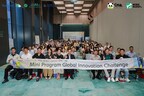
Students tapped on AI tools to build Mini Programs during the Singapore Regional Competition
Hosted by Tencent, the Weixin Mini Program Global Innovation Challenge has grown into a global AI competition for young people internationally since 2022. In over four years, more than 7,000 youth teams worldwide have submitted Mini Program projects, with selected entries advancing to the Weixin Mini Program Global Innovation Challenge Grand Finals held yearly.
In November 2025, the first Weixin Mini Program Global Innovation Challenge (Singapore Regional) competition drew participation from leading schools such as Hwa Chong Institution, Raffles Girls’ School, NUS High School of Mathematics and Science, and Nan Hua High School. Students from Raffles Girls’ School and Nan Hua High School took the Gold Award for their project Singapore: A Fine City, while the competition’s first cross-border team, made up of students from Hwa Chong Institution and Chongqing BI Academy, won the Silver Award for their project, Campus Culture Exchange Station, at the Singapore Regional competition.
Additionally, at the recent 4th Weixin Mini Program Global Innovation Challenge Grand Finals held in Shenzhen in May this year, two Singapore teams secured honours across the top two prize categories, as well as the “Most Valuable Cultural Connection” award. It also recognized Bukit Panjang Government High School as Singapore’s first “Weixin Mini Program AI Education Innovation Base”, where it will integrate the Weixin Mini Program Education Platform into its lower secondary curriculum as part of its interdisciplinary Project-Based Learning (PBL).
On July 21, the Tencent Asia Pacific Management Committee, Singapore’s Association for Research on AI in Learning and Leadership (ARAILL), the Global AI Nexus of Schools (GAINS) and Weixin launched the Weixin Mini Program Global Innovation Challenge (Southeast Asia Regional) Competition. This expanded competition will bring in youth participants from Malaysia, Thailand, and beyond, all competing alongside their global peers to tackle real problems with AI and Mini Programs.
To support the Southeast Asia Regional competition, the Weixin Mini Program Education Platform features a built-in AI assistant that allows students with no prior programming experience to develop practical Mini Programs driven by real-world needs. The platform has already reached nearly 8,000 schools and 87,000 students across 11 countries and regions, hosting more than 287,000 Mini Programs. Through this process of identifying problems, designing solutions, and launching products, students from around the world are provided with AI tools and resources to build Mini Programs that solve everyday problems.
Building Your Own Mini Program: The New “Digital Essential” for Travels
As AI advances and vibe coding goes mainstream, building a Mini Program is now accessible to almost anyone, driving rapid growth across the Weixin ecosystem. Today, Weixin Mini Program services reach over 100 countries and regions, with cross-border and overseas users accessing Mini Programs more than 5 billion times in 2025 alone.
That global reach extends deeply into daily life, where Mini Programs serve as an essential digital guide for Chinese travelers abroad. For instance, Uber, a ride-hailing platform, leverages a Weixin Mini Program to support Chinese tourists across 20 global markets.
In Southeast Asia, Weixin Mini Programs now cover nine markets, including Singapore and Malaysia, with monthly transaction volume surging 160% year on year as of June 2026. From ride-hailing, ticketing, to food delivery, retail, and bike sharing, Mini Programs are rapidly becoming an indispensable digital gateway for both Chinese tourists traveling the region and local consumers in their everyday spending.
In Singapore, Weixin’s “Nearby Services” section puts Mini Programs within easy reach at venues like Changi Airport, the National Gallery Singapore, Marina Bay Sands, and Takashimaya. Resorts World Sentosa has gone a step further, integrating fully with the Weixin ecosystem across eight points of sale with support for Weixin Palm Payment and Mini Program services.
Leveraging Tencent’s AI tools like WorkBuddy and ima
Tencent recently introduced a suite of AI products to international markets, featuring its AI knowledge assistant ima, AI productivity agent WorkBuddy, AI creative studio Miora, and its Model-as-a-Service platform TokenHub. The international version of WorkBuddy features built-in Skills and seamlessly integrates with popular global tools, including WeChat, Slack, Telegram, Discord, GitHub, and Google Drive.
Built around an intelligent knowledge base, ima integrates search, reading, and writing into a unified workflow, ranking first among knowledge-base products in China. It has surpassed 13 million monthly active users, hosts over 420 million knowledge-base files, and operates seamlessly across nine platforms.
To empower young talent abroad to build their own Mini Programs, the Southeast Asia Regional competition leverages Tencent AI tools, including WorkBuddy, ima, and the Weixin Mini Game platform.
These AI tools quickly became a favourite among the student developers on-site at the “AI Agent-themed” Weixin Mini Program competition held during the Southeast Asia Regional launch event ceremony. Students used ima to search, analyze, and save reference material to their personal knowledge bases before leveraging WorkBuddy to build out their concepts. Rather than handing them ready-made answers, the AI serves as an accelerator for critical thinking and inquiry—dramatically shortening the journey from initial research to a fully realized product.
Zoe Chou, Founder of the Weixin Mini Program Global Innovation Challenge, said, “The innovation challenge is not just a coding contest, but a platform to empower students to use AI tools to solve real-world challenges. By bringing the challenge to Southeast Asia, we hope to champion AI education in more schools across the region. Tencent is committed to providing a robust support framework, including tailored teacher training and AI tools, so that young creators can turn their best ideas into reality almost as fast as they can imagine them.”
– Ends –
About Weixin Mini Program Education Platform
The Weixin Mini Program Education Platform, launched by Tencent in 2023, is an AI-enabled platform designed to support education and interdisciplinary project-based learning. It provides teachers and students with a wide range of tools to develop Mini Programs that address real-world problems, while making it easier for educators to organise and guide related learning activities. With a built-in AI assistant, the platform also makes programming more accessible to students with little or no prior coding experience.
About Weixin Mini Program
Weixin Mini Programs are lightweight applications embedded within the Weixin/WeChat app, allowing users to access services easily without downloading a separate app. Officially launched in January 2017, Weixin Mini Programs now serve more than 600 million daily active users worldwide and create over 10 million employment and income-generating opportunities each year. In Singapore, prominent businesses and attractions, including Grab, Changi Airport, Resorts World Sentosa and Mandai Wildlife Reserve, have also launched their own Weixin Mini Programs.
View original content to download multimedia:https://www.prnewswire.com/apac/news-releases/5th-weixin-mini-program-global-innovation-challenge-launches-southeast-asia-regional-competition-inviting-youths-to-build-mini-programs-with-ai-tools-302832926.html
SOURCE Weixin Mini Program


 Technology4 days ago
 Technology5 days ago
 Coin Market3 days ago
 Technology4 days ago
 Technology4 days ago
 Coin Market3 days ago
 Technology3 days ago
 Technology3 days ago