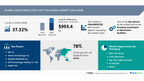
NEW YORK, Oct. 17, 2024 /PRNewswire/ — Report on how AI is driving market transformation – The Global Semiconductor Chip Packaging Market size is estimated to grow by USD 993.4 billion from 2024-2028, according to Technavio. The market is estimated to grow at a CAGR of over 37.32% during the forecast period. Growing investment in fabrication facilities is driving market growth, with a trend towards growing investments in lower technology node. However, high initial investment poses a challenge – Key market players include 3M Co., Amkor Technology Inc., Applied Materials Inc., ASE Technology Holding Co. Ltd., ASMPT Ltd., ChipMOS TECHNOLOGIES INC., Foundaries Inc., Jiangsu Changdian Technology Co. Ltd., Kulicke and Soffa Industries Inc., Microchip Technology Inc., nepes Corp., Powertech Technology Inc., Skywater Technology, SUSS MICROTEC SE, Taiwan Semiconductor Manufacturing Co. Ltd., Tokyo Electron Ltd., Unisem M Berhad, UTAC Holdings Ltd., and Veeco Instruments Inc..
AI-Powered Market Evolution Insights. Our comprehensive market report ready with the latest trends, growth opportunities, and strategic analysis- View your snapshot now
Forecast period
2024-2028
Base Year
2023
Historic Data
2018 – 2022
Segment Covered
Packaging (3DIC TSV stacks, 2.5D interposers, Flip-chip wafer bumping, FO WLP/SiP, and Others), End-user (OSATs and IDMs), and Geography (APAC, North America, Europe, South America, and Middle East and Africa)
Region Covered
APAC, North America, Europe, South America, and Middle East and Africa
Key companies profiled
3M Co., Amkor Technology Inc., Applied Materials Inc., ASE Technology Holding Co. Ltd., ASMPT Ltd., ChipMOS TECHNOLOGIES INC., GlobalFoundaries Inc., Jiangsu Changdian Technology Co. Ltd., Kulicke and Soffa Industries Inc., Microchip Technology Inc., nepes Corp., Powertech Technology Inc., Skywater Technology, SUSS MICROTEC SE, Taiwan Semiconductor Manufacturing Co. Ltd., Tokyo Electron Ltd., Unisem M Berhad, UTAC Holdings Ltd., and Veeco Instruments Inc.
Key Market Trends Fueling Growth
Semiconductor manufacturers are continuously innovating to meet the increasing demand for smaller, more powerful, and energy-efficient semiconductors. To achieve this, they are investing heavily in research and development to identify new technologies, such as FinFET and FD-SOI, for producing ICs with smaller process nodes. Moore’s law, which predicts the number of transistors in an integrated circuit will double approximately every two years, is driving this trend. FinFET and FD-SOI technologies are gaining popularity for their advantages in power consumption, performance, and scalability. FinFET is widely used in 14/16 nm nodes, offering greater density, lower power consumption, and higher performance. FD-SOI technology, used in 10/12 nm nodes, provides a balanced power-performance trade-off and ultra-low power consumption at 0.4V operation. The semiconductor industry is responding by building new fabrication facilities to support the production of ICs based on these lower technology nodes. For instance, Taiwan Semiconductor Manufacturing announced in June 2021 its plan to build an advanced semiconductor fab in the US. The growth in investment in semiconductor manufacturing facilities is expected to fuel the demand for semiconductor chip packaging designed specifically for semiconductor wafers, driving the market’s growth during the forecast period.
The semiconductor chip packaging market is experiencing significant growth due to trends in defense sector spending and the military’s increasing reliance on advanced semiconductor components for defense electronics. IC packaging materials, such as encapsulation resins, leadframes, and thermal interface materials, are in high demand for densifying integrated circuits in military applications. Additionally, the consumer electronics sector, including laptops, smartwatches, and smartphones, is driving demand for miniaturization and advanced packaging solutions like Small Outline Packages and Surface Mount Technology. The 5G revolution and the rise of autonomous vehicles are also fueling growth in this market. Electronics manufacturing hubs are investing in digitalization trends, machine learning, and foreign investments to stay competitive. Advanced packaging technologies like System in Package, 3D packaging, and Organic Substrates are essential for meeting the demands of emerging technologies like Artificial Intelligence, Internet of Things, and Autonomous Driving. However, challenges like product obsolescence, intellectual property concerns, outsourcing, testing processes, and the need for electrical insulation and mechanical support persist. The market is also witnessing the adoption of advanced bonding wire and encapsulation resins for enhanced performance and reliability.
Insights on how AI is driving innovation, efficiency, and market growth- Request Sample!
Market Challenges
The semiconductor chip packaging market is experiencing significant changes due to the increasing demand for compact Integrated Circuits (ICs) and the emergence of advanced packaging solutions like Through-Silicon Vias (TSV), stacked packaging, and Micro-Electromechanical Systems (MEMS) packaging. Manufacturers are investing heavily in new equipment to produce these compact ICs, leading to higher manufacturing costs. The complex manufacturing process, longer production time, and increased risk of defects further add to the expenses. Rapid technological advancements in the semiconductor industry necessitate the use of efficient equipment, increasing the total cost of ownership. Consequently, many companies are adopting a fabless model, reducing the potential customer base for semiconductor chip packaging vendors. Despite the high initial investment, these challenges are expected to hinder market growth during the forecast period.
The semiconductor packaging market is experiencing significant growth due to the increasing demand for advanced technologies in consumer electronics, such as smartphones and tablets. Key sectors driving this growth include electric vehicles, autonomous driving, artificial intelligence, Internet of Things, and advanced packaging. Challenges in semiconductor packaging include miniaturization, thermal and electrical performance, and advanced technologies like System in Package, 3D packaging, organic substrates, and advanced encapsulation resins. Traditional packaging methods like ceramic packages, bonding wire, and die attach materials face competition from advanced techniques like Flip Chip. The aerospace and defense industry, telecommunications market, smart manufacturing, and high-frequency applications also contribute to the market’s growth. Additionally, sectors like automotive electronics, automotive electronics, and wearable technology require advanced packaging solutions for power densities, thermal management, and signal integrity. The market is also impacted by regulations like Production Linked Incentive and the need for electromagnetic interference and electromagnetic compatibility in various applications.
Insights into how AI is reshaping industries and driving growth- Download a Sample Report
Segment Overview
This semiconductor chip packaging market report extensively covers market segmentation by
Packaging 1.1 3DIC TSV stacks1.2 2.5D interposers1.3 Flip-chip wafer bumping1.4 FO WLP/SiP1.5 OthersEnd-user 2.1 OSATs2.2 IDMsGeography 3.1 APAC3.2 North America3.3 Europe3.4 South America3.5 Middle East and Africa
1.1 3DIC TSV stacks- The Semiconductor Chip Packaging Market is experiencing significant growth due to the increasing demand for advanced functionalities, improved performance, and cost reduction. Three-Dimensional Interconnect (3DIC) Through-Silicon Via (TSV) technology is a crucial solution for high-end memory applications, heterogeneous interconnection with CMOS Image Sensors (CIS), micro-electromechanical systems (MEMS), sensors, radio frequency (RF) filters, and performance applications. The popularity of TSV platforms is driven by their ability to increase integration and performance. In the future, TSV technology is expected to be used for applications such as photonics and light-emitting diode (LED) function integration. This trend is anticipated to boost the demand for 3DIC TSV stacks, thereby driving the growth of the Semiconductor Chip Packaging Market during the forecast period.
Download complimentary Sample Report to gain insights into AI’s impact on market dynamics, emerging trends, and future opportunities- including forecast (2024-2028) and historic data (2018 – 2022)
Research Analysis
The Semiconductor Chip Packaging Market encompasses the design, manufacturing, and integration of semiconductor devices into various electronic systems. The market is driven by the increasing demand for consumer electronics, particularly smartphones and tablets, as well as the growing adoption of electric vehicles and autonomous driving technologies. Advanced packaging techniques, such as fan-out wafer level packaging and 2.5D/3D packaging, are gaining popularity due to their ability to increase power densities and improve thermal management in high frequency applications, high performance computing, data processing, and artificial intelligence. Advanced packaging materials, including advanced encapsulation resins, electrical insulation, mechanical support, leadframes, and sensor technologies, play a crucial role in ensuring signal integrity and reliability. Additionally, the market is expanding into new areas such as automotive electronics, advanced driver assistance systems, laptops, smartwatches, and advanced semiconductor components. Integrated cooling mechanisms are becoming increasingly important to address the thermal challenges of these advanced systems.
Market Research Overview
The Semiconductor Chip Packaging Market encompasses various technologies and materials used to protect and connect semiconductor devices in consumer electronics, automotive, aerospace, telecommunications, and other industries. Advanced packaging techniques, such as System in Package (SiP), 3D packaging, and Organic Substrates, are driving innovation in miniaturization, thermal management, and electrical performance. Key applications include smartphones, tablets, electric vehicles, autonomous driving, and the Internet of Things (IoT). Advanced technologies like Artificial Intelligence (AI), Machine Learning (ML), and High Performance Computing (HPC) require advanced semiconductor components and packaging materials for optimal thermal and electrical performance. Traditional packaging methods, such as Ceramic Packages and Die Attach materials, continue to play a role in specific applications, while new materials like advanced encapsulation resins and thermal interface materials offer improved performance and reliability. The market is influenced by trends like smart manufacturing, high frequency applications, and digitalization, as well as challenges like product obsolescence, intellectual property concerns, and testing processes. Emerging applications include autonomous vehicles, 5G, and wearable technology, while industries like defense and military electronics continue to drive demand for advanced semiconductor components and packaging materials. Production-Linked Incentives and Foreign Investments are shaping the market landscape, with electronics manufacturing hubs in Asia, Europe, and North America leading the way.
Table of Contents:
1 Executive Summary
2 Market Landscape
3 Market Sizing
4 Historic Market Size
5 Five Forces Analysis
6 Market Segmentation
Packaging3DIC TSV Stacks2.5D InterposersFlip-chip Wafer BumpingFO WLP/SiPOthersEnd-userOSATsIDMsGeographyAPACNorth AmericaEuropeSouth AmericaMiddle East And Africa
7 Customer Landscape
8 Geographic Landscape
9 Drivers, Challenges, and Trends
10 Company Landscape
11 Company Analysis
12 Appendix
About Technavio
Technavio is a leading global technology research and advisory company. Their research and analysis focuses on emerging market trends and provides actionable insights to help businesses identify market opportunities and develop effective strategies to optimize their market positions.
With over 500 specialized analysts, Technavio’s report library consists of more than 17,000 reports and counting, covering 800 technologies, spanning across 50 countries. Their client base consists of enterprises of all sizes, including more than 100 Fortune 500 companies. This growing client base relies on Technavio’s comprehensive coverage, extensive research, and actionable market insights to identify opportunities in existing and potential markets and assess their competitive positions within changing market scenarios.
Contacts
Technavio Research
Jesse Maida
Media & Marketing Executive
US: +1 844 364 1100
UK: +44 203 893 3200
Email: media@technavio.com
Website: www.technavio.com/
View original content to download multimedia:https://www.prnewswire.com/news-releases/semiconductor-chip-packaging-market-to-grow-by-usd-993-4-billion-from-2024-2028–driven-by-increased-investment-in-fabrication-facilities-and-ai-powered-market-evolution—technavio-302278826.html
SOURCE Technavio


 Technology5 days ago

 Near Videos4 days ago
 Technology5 days ago
 Technology5 days ago
 Technology4 days ago
 Near Videos5 days ago
 Coin Market4 days ago