Connect with us

Technology

Hybrid Bonding Technology Market to Reach USD 756 Million by 2031, Driven by Demand for AI, 5G, and High-Performance Computing | Valuates Reports

Published

on

BANGALORE, India, April 11, 2025 /PRNewswire/ — Hybrid Bonding Technology Market is Segmented by Type (Wafer-to-wafer Hybrid Bonding, Die-to-wafer Hybrid Bonding), by Application (CMOS Image Sensor (CIS), NAND, DRAM, High Bandwidth Memory (HBM)).

The Global Market for Hybrid Bonding Technology was valued at USD 164 Million in the year 2024 and is projected to reach a revised size of USD 756 Million by 2031, growing at a CAGR of 24.7% during the forecast period.

Claim Your Free Report: https://reports.valuates.com/request/sample/QYRE-Auto-26A11376/Global_Hybrid_Bonding_Technology_Market 

Major Factors Driving the Growth of Hybrid Bonding Technology Market:

The Hybrid Bonding Technology Market is transitioning from early‑adopter phase to high‑growth mainstream adoption. Capacity announcements, multi‑year equipment backlogs, and expanding design‑win pipelines signal robust double‑digit revenue growth through the forecast horizon. As heterogeneous integration becomes indispensable for AI, 5G, automotive autonomy, and ultra‑high‑resolution imaging, hybrid bonding emerges as the de facto interconnect standard, eclipsing micro‑bump and TSV‑centric approaches. Continued process refinements and cost reductions will open mid‑tier and IoT segments, further enlarging addressable demand. Overall, hybrid bonding stands poised to redefine advanced packaging economics and performance benchmarks, anchoring a vibrant ecosystem of materials, tools, and service providers.

Unlock Insights: View Full Report Now! https://reports.valuates.com/market-reports/QYRE-Auto-26A11376/global-hybrid-bonding-technology

TRENDS INFLUENCING THE GROWTH OF THE HYBRID BONDING TECHNOLOGY MARKET:

Wafer‑to‑wafer hybrid bonding is emerging as a pivotal manufacturing step because it enables full‑surface metal‑oxide interconnects that virtually eliminate the parasitic resistance and capacitance associated with‑silicon vias. By stacking fully processed wafers with nanometer‑level alignment accuracy, manufacturers can co‑integrate logic, memory, photonic, and sensor layers into one monolithic three‑dimensional package, delivering massive bandwidth and lower energy per bit. These measurable system advantages have made wafer‑to‑wafer architectures indispensable for high‑performance computing, mobile processors, and AI accelerators, spurring capacity expansions by foundries and OSATs. Equipment vendors are likewise benefiting, booking orders for plasma activation tools, bonding aligners, and cluster systems. The resulting cycle of demand, investment, and ecosystem maturation propels sustained, robust growth in the Hybrid Bonding Technology Market worldwide today.

Die‑to‑wafer hybrid bonding unlocks heterogeneous integration by allowing known‑good die from disparate process nodes to be placed precisely onto a target wafer, eliminating costly yield penalties linked with full wafer stacking. This pick‑and‑place flexibility lets designers mix advanced logic, high‑density memory, and specialty analog functions inside a single 3D package, tailoring performance while shrinking footprint. The approach is particularly attractive for chiplet architectures powering data‑center GPUs, network switches, and AI accelerators where interposer limitations bottleneck bandwidth. As system companies embrace the chiplet paradigm, demand for die‑to‑wafer processes is skyrocketing, prompting capital spending on bond aligners, plasma cleaners, and metrology. Collaborative standards such as UCIe reinforce ecosystem confidence, amplifying orders. Consequently, die‑to‑wafer adoption expands revenue within the Hybrid Bonding Technology Market.

CMOS Image Sensors (CIS) are driving a share of hybrid bonding demand because the technology dramatically improves pixel‑level interconnect density, enabling smaller pitch, higher resolution, and superior signal‑to‑noise ratios. By hybrid‑bonding the photodiode wafer to a dedicated logic wafer, manufacturers separate light‑sensitive and processing functions, maximizing fill factor while embedding advanced AI engines beneath each pixel. This architecture is essential for smartphone cameras, automotive ADAS modules, security systems, and emerging AR/VR devices that require multi‑megapixel performance without thermal or power penalties. Major CIS foundries in Japan, South Korea, and Taiwan are investing heavily in hybrid bonding lines, negotiating long‑term supply agreements with handset and automotive OEMs. Their outlays translate into expanding tool shipments, bolstering Hybrid Bonding Technology Market growth trajectories.

Data‑center operators and cloud service providers are deploying ever‑larger AI training clusters and exascale supercomputers that crave higher memory bandwidth, lower latency, and reduced power consumption. Traditional 2.5D interposers and wire‑bonded packages cannot keep pace with the throughput requirements of transformer models and graph analytics. Hybrid bonding overcomes these bottlenecks by providing direct copper‑to‑copper interconnects at pitches below ten microns, allowing logic and HBM stacks to exchange terabytes per second while staying within stringent energy budgets. As hyperscalers commit billions to next‑gen accelerators, they push chip suppliers toward aggressive adoption roadmaps, thereby amplifying equipment, material, and service revenues across the Hybrid Bonding Technology ecosystem worldwide. The virtuous demand cycle intensifies competition and innovation momentum further.

Consumers expect thinner smartphones, smartwatches, and augmented reality glasses that deliver desktop‑class functionality without sacrificing battery life. Achieving such compactness requires stacking logic, memory, RF front‑ends, and power management circuits vertically rather than expanding the PCB footprint. Hybrid bonding enables this architecture by allowing fine‑pitch interconnects between heterogeneous wafers and dies, eliminating the height penalties of micro‑bumps. OEM roadmaps from Silicon Valley to Shenzhen explicitly reference hybrid bonding for next‑generation application processors and camera modules, triggering early production ramps at foundries. Component miniaturization also frees board area for larger batteries and novel sensors, creating additional differentiation. Consequently, handset competition acts as a persistent catalyst that widens the addressable Hybrid Bonding Technology Market, boosting volume shipments.

Automotive OEMs are integrating lidar, radar, high‑resolution cameras, and domain controllers to achieve advanced driver‑assistance and eventual autonomous operation. These sensor arrays generate enormous data streams that must be processed in real‑time under harsh thermal and vibration conditions. Hybrid bonding facilitates compact, ruggedized 3D stacks that combine logic, memory, and sensor dies, improving bandwidth and reducing latency while maintaining reliability. Government safety regulations such as Euro NCAP and China NCAP push adoption of ADAS features, creating predictable, multi‑year demand for high‑performance automotive semiconductors. Tier‑1 suppliers consequently sign capacity reservations with foundries, driving equipment purchases for hybrid bonding lines and reinforcing market growth.

 Initial hybrid bonding lines suffered from particle‑induced voids and alignment errors, but iterative advances in plasma activation chemistry, wafer‑handling robotics, and in‑line inspection have driven dramatic yield gains. Higher yields translate directly into lower cost‑per‑connection, making hybrid bonding economically competitive with micro‑bump solutions at high volumes. OSATs now advertise greater than 99 percent bonding yield for both wafer‑to‑wafer and die‑to‑wafer flows, convincing cautious fabless customers to convert existing 2.5D programs. As unit costs fall, hybrid bonding becomes viable for mid‑range mobile and IoT chips, expanding the addressable market. Continuous process optimization therefore serves as a reinforcing growth driver, unlocking new design‑win opportunities.

Claim Yours Now! https://reports.valuates.com/api/directpaytoken?rcode=QYRE-Auto-26A11376&lic=single-user

HYBRID BONDING TECHNOLOGY MARKET SHARE:

Asia‑Pacific dominates the Hybrid Bonding Technology Market, led by Taiwan’s advanced‑node foundries, South Korea’s memory giants, and Japan’s CMOS image‑sensor specialists. China is rapidly scaling domestic capacity through state‑backed programs, while Southeast Asia’s OSAT clusters in Singapore and Malaysia add assembly breadth. North America follows, buoyed by U.S. logic IDMs and government‑funded packaging pilot lines. Europe leverages research institutes and automotive demand, whereas Israel anchors niche aerospace and defense applications.

Key Companies:

IntelApplied MaterialsHuaweiEV Group (EVG)SUSS MicroTecAdeia

Purchase Regional Report: https://reports.valuates.com/request/regional/QYRE-Auto-26A11376/Global_Hybrid_Bonding_Technology_Market 

SUBSCRIPTION

We have introduced a tailor-made subscription for our customers. Please leave a note in the Comment Section to know about our subscription plans.

DISCOVER MORE INSIGHTS: EXPLORE SIMILAR REPORTS!

–          Hybrid Bonding Equipment Market was valued at USD 123 Million in the year 2023 and is projected to reach a revised size of USD 618 Million by 2030, growing at a CAGR of 24.7% during the forecast period.

–          Wafer Hybrid Bonding Equipment Market was valued at USD 164 Million in the year 2024 and is projected to reach a revised size of USD 756 Million by 2031, growing at a CAGR of 24.7% during the forecast period.

–          Wafer Bonding Equipment Market was valued at USD 321 Million in the year 2024 and is projected to reach a revised size of USD 449 Million by 2031, growing at a CAGR of 5.0% during the forecast period.

–          Hybrid Wedge Bonders market was valued at USD 54 Million in 2023 and is anticipated to reach USD 70 Million by 2030, witnessing a CAGR of 3.0% during the forecast period 2024-2030.

–          Chip Bonding Adhesive Market was valued at USD 355 Million in the year 2023 and is projected to reach a revised size of USD 510 Million by 2030, growing at a CAGR of 5.3% during the forecast period.

–          Optical Bonding Service Market

–          Temporary Bonding and Debonding Systems Market

–          Wafer Bond Alignment System Market was valued at USD 249 Million in the year 2023 and is projected to reach a revised size of USD 423 Million by 2030, growing at a CAGR of 7.9% during the forecast period.

–          Die Bonding Materials Market

–          Automotive Glass Bonding Market

–          Bonding Wire for Semiconductor Packaging Market

DISCOVER OUR VISION: VISIT ABOUT US!

Valuates offers in-depth market insights into various industries. Our extensive report repository is constantly updated to meet your changing industry analysis needs.

Our team of market analysts can help you select the best report covering your industry. We understand your niche region-specific requirements and that’s why we offer customization of reports. With our customization in place, you can request for any particular information from a report that meets your market analysis needs.

To achieve a consistent view of the market, data is gathered from various primary and secondary sources, at each step, data triangulation methodologies are applied to reduce deviance and find a consistent view of the market. Each sample we share contains a detailed research methodology employed to generate the report. Please also reach our sales team to get the complete list of our data sources.

GET A FREE QUOTE
Valuates Reports
sales@valuates.com
For U.S. Toll-Free Call 1-(315)-215-3225
WhatsApp: +91-9945648335
Website: https://reports.valuates.com
Blog: https://valuatestrends.blogspot.com/
Pinterest: https://in.pinterest.com/valuatesreports/
Twitter: https://twitter.com/valuatesreports
Facebook: https://www.facebook.com/valuatesreports/
YouTube: https://www.youtube.com/@valuatesreports6753
https://www.facebook.com/valuateskorean
https://www.facebook.com/valuatesspanish
https://www.facebook.com/valuatesjapanese
https://valuatesreportspanish.blogspot.com/
https://valuateskorean.blogspot.com/
https://valuatesgerman.blogspot.com/
https://valuatesreportjapanese.blogspot.com/ 

Logo: https://mma.prnewswire.com/media/1082232/Valuates_Reports_Logo.jpg


View original content:https://www.prnewswire.co.uk/news-releases/hybrid-bonding-technology-market-to-reach-usd-756-million-by-2031-driven-by-demand-for-ai-5g-and-high-performance-computing–valuates-reports-302426561.html

Continue Reading
Click to comment

Leave a Reply

Your email address will not be published. Required fields are marked *

Technology

As ADA Anniversary Approaches, University of Phoenix Survey Highlights AI’s Potential to Advance Accessibility in Work and Learning

Published

on

By

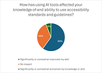
Survey conducted by The Harris Poll on behalf of University of Phoenix finds among those already using AI in the workplace, 60% say AI has improved their knowledge of and ability to use accessibility standards and guidelines.

PHOENIX, July 24, 2026 /PRNewswire/ — As artificial intelligence becomes part of how people work, learn and solve problems, a new University of Phoenix survey conducted by The Harris Poll finds that recent working learners see meaningful opportunities for AI to support accessibility. The survey was designed to understand the impact of AI in the workplace and learning environments on accessibility, defined as ensuring digital content, tools and resources, including AI tools and output, are usable by people with different abilities through inclusive design, use of assistive technology or conformance with accessibility standards, such as the Web Content Accessibility Guidelines (WCAG). The findings are being released ahead of the 36th anniversary of the Americans with Disabilities Act (ADA) on July 26.

The survey, conducted among 1,019 U.S. employed adults who completed a professionally presented training or school course in the past 12 months (“recent working learners”), found that, among workers already using AI in the workplace, 3 in 5 (60%) say AI has improved their knowledge of and ability to use accessibility standards and guidelines, including nearly 1 in 5 (19%) who report significant improvement. 

While the findings point to optimism about AI’s accessibility potential, they also reveal an opportunity for clearer organizational guidance: 45% of respondents say accessibility is absent from, unclear in, or they are uncertain whether it is covered by their workplace AI policies.

“The reality is that accessibility benefits everyone,” shares Kelly Hermann, Vice President of Accessibility and Student Affairs at University of Phoenix. “If accessibility is built in from the beginning, organizations are more likely to create AI-enabled environments that are universally usable. Clearer content, better summaries, accurate captions, and multiple formats can help workers and learners with disabilities, but they also help busy adults, multilingual learners, mobile users, and anyone trying to absorb information quickly.”

Key findings from the survey include:

Workers see AI’s accessibility potential: 89% of recent working learners identify workflows that could benefit from AI and accessibility tools, especially creating accessible documents, presentations, websites or learning materials (38%), presenting information in different formats such as plain language, audio, summaries or translations (33%), and training employees or learners on accessibility practices (30%).AI may help build accessibility awareness: Among those already using AI in the workplace, 60% say AI has improved their knowledge of and ability to use accessibility standards and guidelines.Accessibility is not always clear in workplace AI policies: 45% of recent working learners say accessibility is absent from, unclear in, or they are uncertain whether it is covered by their workplace AI policies.AI tools may not yet fully support different access needs: Among those who use workplace AI tools, only about a quarter of survey respondents (27%) say AI tools available through their workplace or professional learning environment support people with disabilities very well.Human oversight remains important: 36% of recent working learners say human review for important decisions or high-impact work should be part of responsible AI use at work or school.Workers also recognize how AI and accessibility can have an impact on their own career journey: 90% of recent working learners identify AI and accessibility skills that would be valuable in their current or desired career field, including 45% who see value in understanding when AI-generated content needs human review.

Why accessibility is essential to responsible AI adoption

As AI tools are used to draft documents, summarize information, generate captions and transcripts, create image descriptions, support learning and assist with workplace tasks, accessibility becomes central to responsible use. Poorly implemented AI can also create or amplify barriers, including inaccessible content, inaccurate summaries, biased outputs and tools that do not work effectively with assistive technologies.

“Responsible AI is not only about productivity,” Hermann said. “It is about whether the technology works for the people who need to use it. AI can help create more accessible materials and more flexible ways to engage with information, but it still requires clear policies, practical training and human judgment to make sure the outputs are accurate, applicable and usable.”

What the findings mean for employers and educators

The survey suggests that organizations have an opportunity to align AI adoption with supportive design, accessibility practices and workforce training. Employers and educators can take immediate steps by:

Naming accessibility directly in AI policies and guidance.Choosing AI tools with accessibility and assistive technology compatibility in mind.Training workers and learners to create, check and improve accessible AI-generated content.Making support pathways clear for people who experience barriers using AI tools.Keeping human review in place for important decisions, high-impact work and accessibility-sensitive outputs.

The survey also found workers want practical AI training. The most helpful resources identified by recent working learners include real-world examples from their field or industry (36%), hands-on practice using realistic workplace scenarios (34%) and step-by-step demonstrations of common tasks (33%).

Accessibility insights from University of Phoenix

Hermann shared the survey findings ahead of the ADA anniversary in recent media interviews. Hermann oversees the University’s accessibility initiative, including evaluation and remediation of curricular resources, the Center for Access, Resources, Engagement and Support Services (CARES), and the Office of Collaborative Learning and Educational Engagement. Her work focuses on fostering accessible and welcoming educational environments for students, faculty and staff.

Hermann’s office at University of Phoenix also convenes accessibility conversations through initiatives such as Access Amplified™, a free, annual virtual event focused on advancing digital accessibility in web development. The event brings together engineers, developers, designers, content authors and digital strategists for practical strategies and human-centered conversations that address the gap between coding practices and how users with assistive technology experience the web.

About the survey

The survey was conducted online within the United States by The Harris Poll on behalf of University of Phoenix from June 22–29, 2026, among 1,019 employed adults ages 18 and older who have taken a professionally presented training or a school course in the past 12 months, referred to as “recent working learners.” Data were weighted where necessary by age, gender, race/ethnicity, region, education, employment, marital status, household size, household income and smoking status to bring them in line with their actual proportions in the population.

Respondents for this survey were selected from among those who have agreed to participate in surveys. The sampling precision of Harris online polls is measured by using a Bayesian credible interval. For this study, the sample data is accurate to within +/- 3.8 percentage points using a 95% confidence level. This credible interval will be wider among subsets of the surveyed population of interest.

Review the complete survey at phoenix.edu/aiaccessibility.

About University of Phoenix

University of Phoenix is Built for Real Life. 50 Years Strong. The University innovates to help working adults enhance their careers and develop skills in a rapidly changing world through flexible online learning, relevant courses, academic AI pillars, and skills-mapped curriculum for associate, bachelor’s and master’s degree programs. Active students and alumni have access to Career Services for Life® resources including career guidance and tools. For more information, visit phoenix.edu. 

View original content to download multimedia:https://www.prnewswire.com/news-releases/as-ada-anniversary-approaches-university-of-phoenix-survey-highlights-ais-potential-to-advance-accessibility-in-work-and-learning-302834448.html

SOURCE University of Phoenix

Continue Reading

Technology

Mastech Digital to Announce Second Quarter 2026 Financial Results; Participate in Upcoming Investor Conference

Published

on

By

PITTSBURGH, July 24, 2026 /PRNewswire/ — Mastech Digital, Inc. (NYSE American: MHH) (“Mastech Digital”), a leading provider of Digital Transformation IT Services, today announced the date for the release of its financial results for the second quarter ended June 30, 2026, and its participation in an upcoming investor conference.

Second Quarter 2026 Earnings:

Mastech Digital will report its financial results for the second quarter 2026 before the market opens on Thursday, August 6, 2026. Management will host a live conference call and webcast at 9:00 a.m. Eastern Time on that day to discuss the Company’s financial performance and operating results.  The conference call will be hosted by Nirav Patel, President and CEO, and Kannan Sugantharaman, Chief Financial and Operations Officer.

Those wishing to participate via webcast should access the call through Mastech Digital’s Investor Relations website at https://investors.mastechdigital.com. Those wishing to participate via telephone may dial in at 1-800-715-9871 (USA) or 1-646-307-1963 (International) with the passcode 7506988. The replay will be available via webcast through Mastech Digital’s Investor Relations website.

Upcoming Investor Conference:

Mr. Sugantharaman will host a fireside chat at the Sidoti Micro-Cap Investor Conference on Wednesday, August 19, 2026, at 9:15 a.m. Eastern Time.

Mastech Digital management is scheduled to host virtual one-on-one and small group meetings with investors during the conference on August 19-20, 2026. Investors interested in arranging a meeting should contact their Sidoti representative or reach out to the Mastech Digital investor relations team at investors@mastechdigital.com.

About Mastech Digital, Inc.

Mastech Digital (NYSE American: MHH) is a leading provider of Digital Transformation IT Services. The Company offers Data Management, Analytics & AI Solutions, and IT Staffing Services with a digital-first approach. A minority-owned enterprise, Mastech Digital is headquartered in Pittsburgh, PA, with offices across the U.S., Canada, Europe, and India. Visit us at www.mastechdigital.com.

Investor Relations Contact:
investors@mastechdigital.com 


View original content to download multimedia:https://www.prnewswire.com/news-releases/mastech-digital-to-announce-second-quarter-2026-financial-results-participate-in-upcoming-investor-conference-302834421.html

SOURCE Mastech Digital, Inc.

Continue Reading

Technology

SOLAI Limited Announces Extraordinary General Meeting

Published

on

By

AKRON, Ohio, July 24, 2026 /PRNewswire/ — SOLAI Limited (NYSE: SLAI) (“SOLAI” or the “Company”) (previously known as “BIT Mining Limited”), a technology-driven personal AI and digital infrastructure provider, today announced that it will hold its extraordinary general meeting of shareholders at 428 South Seiberling Street, Akron, Ohio, US on August 14, 2026 at 10:00 a.m., New York time.

Holders of record of ordinary shares and preference shares of the Company at the close of business on July 20, 2026, New York time (the “Record Date”) are entitled to receive notice of, and to attend and vote at, the extraordinary general meeting or any adjournment thereof. Holders of the Company’s American Depositary Shares (“ADSs”) who wish to exercise their voting rights for the underlying ordinary shares must act through the depositary of the Company’s ADS program, Deutsche Bank Trust Company Americas.

The notice of the extraordinary general meeting, which sets forth the resolutions to be submitted to shareholder approval at the extraordinary general meeting is available on the Investor Relations section of the Company’s website at https://ir.solai.com

About SOLAI Limited

SOLAI Limited (previously known as “BIT Mining Limited”) (NYSE: SLAI) (previously traded under “BTCM”) is a technology-driven personal AI and digital infrastructure provider. Building upon its historical legacy in digital asset mining and blockchain network operations, the Company is leveraging extensive experience in large-scale hardware deployment, data center operations, and high-performance computing to build the foundational infrastructure for personal AI computing and digital asset ecosystems globally.

For more information:

SOLAI Limited
ir@solai.com
ir.solai.com
www.solai.com 

Christensen Advisory
Jason Ng
Tel: +852-2117-0861
Email: solai@christensencomms.com 


View original content:https://www.prnewswire.com/news-releases/solai-limited-announces-extraordinary-general-meeting-302834034.html

SOURCE SOLAI Limited

Continue Reading

Trending