Connect with us

Technology

Semiconductor Market to Grow by USD 157.1 Billion by 2029, Growing Adoption of IoT Devices Boosts Market, Report on How AI is Redefining the Landscape – Technavio

Published

on

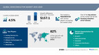
NEW YORK, Feb. 6, 2025 /PRNewswire/ — Report with market evolution powered by AI – The global semiconductor market size is estimated to grow by USD 157.1 billion from 2025-2029, according to Technavio. The market is estimated to grow at a CAGR of 4.5% during the forecast period. Growing adoption of iot devices is driving market growth, with a trend towards increasing adoption of sustainability manufacturing. However, supply-demand gap in global semiconductor market poses a challenge. Key market players include Analog Devices Inc., Broadcom Inc., Infineon Technologies AG, Intel Corp., MediaTek Inc., Microchip Technology Inc., Micron Technology Inc., NVIDIA Corp., NXP Semiconductors NV, ON Semiconductor Corp., Qualcomm Inc., Renesas Electronics Corp., Samsung Electronics Co. Ltd., Skyworks Solutions Inc., Sony Group Corp., STMicroelectronics NV, Taiwan Semiconductor Manufacturing Co. Ltd., Texas Instruments Inc., Toshiba Corp., and Wolfspeed Inc.

Key insights into market evolution with AI-powered analysis. Explore trends, segmentation, and growth drivers- View Free Sample PDF

Semiconductor Market Scope

Report Coverage

Details

Base year

2024

Historic period

2019 – 2023

Forecast period

2025-2029

Growth momentum & CAGR

Accelerate at a CAGR of 4.5%

Market growth 2025-2029

USD 157.1 billion

Market structure

Fragmented

YoY growth 2022-2023 (%)

3.6

Regional analysis

APAC, North America, Europe, South America, and Middle East and Africa

Performing market contribution

APAC at 82%

Key countries

China, US, Germany, Canada, Taiwan, South Korea, Japan, India, UK, and France

Key companies profiled

Analog Devices Inc., Broadcom Inc., Infineon Technologies AG, Intel Corp., MediaTek Inc., Microchip Technology Inc., Micron Technology Inc., NVIDIA Corp., NXP Semiconductors NV, ON Semiconductor Corp., Qualcomm Inc., Renesas Electronics Corp., Samsung Electronics Co. Ltd., Skyworks Solutions Inc., Sony Group Corp., STMicroelectronics NV, Taiwan Semiconductor Manufacturing Co. Ltd., Texas Instruments Inc., Toshiba Corp., and Wolfspeed Inc.

Market Driver

The semiconductor market is experiencing significant trends driven by artificial intelligence, Internet of Things, and machine learning. According to IDC, the semiconductor industry is projected to grow, with B2B enterprises, B2G enterprises, and B2C enterprises driving demand. Integrated circuits, including memory chips, PC sales, smartphones, data center chips, and communication components, are key areas of focus. Semiconductor companies like Navitas Semiconductor and Polymatech Electronics are making strides in AI semiconductors, while ASE/SPIL, Amkor, and others lead in manufacturing. VR, 5G, and 6G are emerging technologies driving progress and breakthroughs in semiconductor devices. Affordability, dependability, and compact size are essential factors for diverse electronics. In the forthcoming years, there will be a rising need for semiconductors in autonomous driving, electrification, and automation. The telecom sector, automotive, consumer electronics, IT and communications, healthcare, aerospace and defense, and consumer goods are major markets. Semiconductor materials, including silicon, gallium arsenide, and emerging materials like aluminum nitride and carbon nanotubes, are crucial for advanced microelectronics and high-end data centers. The fab utilization rate is a critical factor for profitable operations, with intense competition and widespread adoption driving changes in demand and customer behavior. Capital investments and skilled workers are essential for manufacturing capacity constraints and post-pandemic era challenges. 

The semiconductor industry faces significant challenges in meeting the increasing demand for semiconductors due to emerging technologies such as 5G, Artificial Intelligence (AI), and the Internet of Things (IoT). One semiconductor fabrication plant consumes approximately 1 Terawatt-hour (TWh) of energy per year and requires two-to-four million gallons of ultra-pure water daily. To address these concerns, industry leaders like Taiwan Semiconductor Manufacturing Company, Limited (TSMC) and Intel Corporation (Intel) are implementing sustainability programs. TSMC is focusing on water recycling applications, expanding diverse water sources, and developing pollution prevention techniques to optimize water usage efficiency. Similarly, Intel is investing in renewable energy and water conservation initiatives to reduce their environmental footprint. These efforts aim to minimize the environmental impact of semiconductor manufacturing while maintaining production capacity to meet the growing demand for these essential technologies. 

Request Sample of our comprehensive report now to stay ahead in the AI-driven market evolution!

Market Challenges

The semiconductor market is facing significant challenges from emerging technologies such as artificial intelligence, Internet of Things, and machine learning. According to IDC, the semiconductor industry is expected to grow in the forthcoming years due to the rising need for electronics in various sectors like B2B enterprises, B2G enterprises, and B2C enterprises. However, this growth comes with challenges such as affordability, dependability, and compact size. Semiconductor companies are investing heavily in AI semiconductors for smart manufacturing and generative AI accelerators. The chip industry is also focusing on 5G and 6G, VR, and autonomous driving. The semiconductor industry association reports that there is intense competition and widespread adoption of electrification, autonomy, and electrification in automotive, consumer electronics, IT and communications, healthcare, aerospace and defense, and more. The semiconductor market includes discrete semiconductors, semiconductor devices, and semiconductor materials segments. The semiconductor devices segment includes power-efficient devices for wireless and portable electronic products, efficient power management, and system architectures. The semiconductor materials segment includes advanced microelectronics, high-end data centers, and automotive applications. Manufacturing capacity constraints, changes in demand, and customer behavior are impacting business revenues and corporate operations. Lead times, capital investments, and skilled workers are essential parts of the supply side. Export controls, cyberattacks, and node manufacturing equipment are also challenges for semiconductor companies. The post-pandemic era will bring changes in demand for essential parts like MOSFET, telecom sector switching power supply, power semiconductors, and IGBT. The semiconductor industry is continuously evolving with contemporary technology, progress, and breakthroughs in subsequent technologies like gallium arsenide, aluminum nitride, and carbon nanotubes. Semiconducting materials like silicon, process chemicals, photomasks, electronic gases, and photoresist ancillaries are crucial for fabrication.The semiconductor market has seen significant growth due to increasing demand from various sectors. Connected devices, artificial intelligence, machine learning, data centers, and smart technologies are key drivers. This demand has resulted in semiconductor supply shortages and longer lead times, causing price increases. Manufacturers face challenges meeting demand, leading to delayed chip deliveries. These price hikes can impact profit margins for manufacturers and raise costs for end-users, potentially influencing consumer spending on electronics.

Discover how AI is revolutionizing market trends- Get your access now!

Segment Overview 

This semiconductor market report extensively covers market segmentation by

ApplicationN And CData ProcessingIndustrialConsumer ElectronicsOthersProductICsOptoelectronicsDiscrete SemiconductorsSensorsGeographyAPACNorth AmericaEuropeSouth AmericaMiddle East And AfricaSemiconductor MaterialsFabricationPacakging

1.1 N and C- The Networking and Communication (N&C) segment is a substantial part of the global semiconductor market, comprising various semiconductor devices and components used in communication technologies and networking infrastructures. With the world’s increasing connectivity and reliance on efficient communication, the demand for semiconductor solutions in this segment continues to expand. The proliferation of smartphones, tablets, laptops, IoT devices, and other connected devices has in data demand. Consumers and businesses require faster and more reliable communication, driving the need for advanced semiconductor solutions that support high-speed data transmission. The rollout of 5G technology is a significant growth driver, promising higher data speeds and lower latency, enabling new applications and services like enhanced mobile connectivity. 5G networks necessitate a multitude of semiconductor components, such as RF front-end modules, baseband processors, and antennas, fueling the demand for communication ICs. Additionally, the increasing popularity of IoT devices and applications, including smart homes and industrial sensors, heavily relies on semiconductor solutions for wireless connectivity, data processing, and energy efficiency. The growing trend of video streaming, online gaming, and social media platforms puts immense pressure on network bandwidth. Semiconductor solutions are crucial in ensuring efficient and reliable transmission of video content. Consequently, the escalating demand for semiconductors is anticipated to propel the expansion of the N&C segment of the global semiconductor market during the forecast period.

Download a Sample of our comprehensive report today to discover how AI-driven innovations are reshaping competitive dynamics

Research Analysis

The semiconductor market is experiencing significant growth due to the increasing demand for contemporary technology in various industries. Artificial intelligence and the Internet of Things are driving the market, with machine learning algorithms requiring advanced semiconductor devices for processing and analysis. According to IDC, the global semiconductor market is expected to reach USD1.1 trillion by 2026, driven by B2B enterprises, B2G enterprises, and B2C enterprises. Integrated circuits, memory chips, computer chips, data center chips, and communication chips are in high demand. Inventories are being managed carefully to ensure profitable fab utilization, with VAT and Spring being key considerations. Semiconductors are essential electronic components made from semiconducting materials, including transistors and diodes. Breakthroughs in semiconductor technology continue to pave the way for subsequent technologies, revolutionizing industries and transforming our daily lives.

Market Research Overview

The semiconductor market is experiencing significant growth in the contemporary technology landscape, driven by emerging technologies such as Artificial Intelligence (AI), Internet of Things (IoT), and Machine Learning. The IDC forecasts expansion of the semiconductor industry in the forthcoming years, with the level of digitization, GDP, exchange rates, and changes in demand playing crucial roles. Integrated Circuit (IC) manufacturers cater to various sectors, including B2B enterprises, B2G enterprises, and B2C enterprises. Semiconductor devices, including memory chips, communication chips, data center chips, and power semiconductors, are essential components for diverse electronics. The semiconductor industry is witnessing intense competition, with companies focusing on affordability, dependability, compact size, and utilization. The chip industry is also investing in IP and cybersecurity to counteract cyberattacks and export controls. Semiconductor manufacturing involves advanced microelectronics, process chemicals, photomasks, and other materials. The Fabrication segment includes high-energy power-efficient devices, wireless and portable electronic products, efficient power management, and system architectures. The Semiconductor Materials Segment encompasses advanced materials like gallium arsenide, silicon, and emerging materials like aluminum nitride and carbon nanotubes. The semiconductor industry’s progress is marked by breakthroughs and subsequent technologies, such as VR, 5G, and 6G. The industry is also addressing challenges like manufacturing capacity constraints, lead times, and capital investments. The post-pandemic era will bring changes in demand, shortages, and customer behavior, impacting business revenues and corporate operations. The semiconductor industry serves various sectors, including automotive, consumer electronics, IT and communications, healthcare, aerospace and defense, and more. Companies like Navitas Semiconductor, Polymatech Electronics, ASE/SPIL, Amkor, and others are key players in the industry, focusing on AI semiconductors, smart manufacturing, and other innovative technologies. The industry’s future is promising, with a sustainable focus on electrification, autonomy, and a profitable path towards a smart manufacturing ecosystem.

Table of Contents:

1 Executive Summary
2 Market Landscape
3 Market Sizing
4 Historic Market Size
5 Five Forces Analysis
6 Market Segmentation

ApplicationN And CData ProcessingIndustrialConsumer ElectronicsOthersProductICsOptoelectronicsDiscrete SemiconductorsSensorsGeographyAPACNorth AmericaEuropeSouth AmericaMiddle East And AfricaSemiconductor MaterialsFabricationPacakging

7 Customer Landscape
8 Geographic Landscape
9 Drivers, Challenges, and Trends
10 Company Landscape
11 Company Analysis
12 Appendix

About Technavio

Technavio is a leading global technology research and advisory company. Their research and analysis focuses on emerging market trends and provides actionable insights to help businesses identify market opportunities and develop effective strategies to optimize their market positions.

With over 500 specialized analysts, Technavio’s report library consists of more than 17,000 reports and counting, covering 800 technologies, spanning across 50 countries. Their client base consists of enterprises of all sizes, including more than 100 Fortune 500 companies. This growing client base relies on Technavio’s comprehensive coverage, extensive research, and actionable market insights to identify opportunities in existing and potential markets and assess their competitive positions within changing market scenarios.

Contacts

Technavio Research
Jesse Maida
Media & Marketing Executive
US: +1 844 364 1100
UK: +44 203 893 3200
Email: media@technavio.com
Website: www.technavio.com/

View original content to download multimedia:https://www.prnewswire.com/news-releases/semiconductor-market-to-grow-by-usd-157-1-billion-by-2029–growing-adoption-of-iot-devices-boosts-market-report-on-how-ai-is-redefining-the-landscape—technavio-302368513.html

SOURCE Technavio

Continue Reading
Click to comment

Leave a Reply

Your email address will not be published. Required fields are marked *

Technology

American Binary Sets New Standard in Post-Quantum Cryptographic VPNs with Symbolic Proof and Attestation

Published

on

By

WASHINGTON, July 21, 2026 /PRNewswire/ — American Binary, a leader in deep-tech cybersecurity, today announced an independent attestation regarding the validity of all 120 security properties of MaxKyber, their network protocol at the heart of their Ambit Client enterprise VPN, now third-party verified to comply with all Commercial National Security Algorithm Suite 2.0 (CNSA 2.0) requirements. This landmark verification is the result of an exhaustive private peer-review of their symbolic proof (Tamarin + ProVerif) and engineering documentation conducted by industry luminaries Dr. Joe Kiniry, PhD and Dr. Tom Shrimpton, PhD, both with long careers in academia and industry, including time at Galois as Principal Scientists.

“No known VPN — post-quantum or classical, deployed or research — has been subjected to specification and formal verification of comparable depth.” – Dr. Joe Kiniry, PhD and Dr. Tom Shrimpton, PhD

In a landscape defined by emerging quantum threats and unproven solutions, this formal third-party verification differentiates MaxKyber from traditional or hybrid solutions by providing certainty in engineering and compliance with National Security requirements. MaxKyber provides the world with long-term full post-quantum security unlike shorter-term temporary solutions such as hybrids (which mix classical and post-quantum encryption). This breakthrough marks a transition from speculative security to a foundation of verified, provable resilience, establishing a new global benchmark for secure communications.

“While organizations today are increasingly recognizing the significance of PQC, American Binary has been preparing for a post-quantum world for seven years. The result is a resilient foundation for secure operations, today and in the post‑quantum future” – Oracle

Additionally, American Binary signed ACM Turing Award winner Whitfield Diffie, cryptographic pioneer and co-inventor of the Diffie-Hellman key exchange, as a key advisor. Whitfield joins the ranks of existing cryptographic advisors Bruce Schneier and Brian LaMacchia.

“Buy American Binary and you’ll be safe”

– Whitfield Diffie at Quantum.Tech World 2026

Key security pillars of the MaxKyber attestation include:

Protection against “Harvest Now, Decrypt Later” (HNDL): By utilizing purely CNSA 2.0 algorithms, including ML-KEM-1024 without any classical key exchange variants, MaxKyber secures today’s data against decryption by quantum adversaries.Comprehensive Symbolic Verification: The attestation covers 120 security properties across 11 critical categories, including secrecy, authentication, forward secrecy, identity hiding, and resistance to Replay, Denial of Service, Resource Exhaustion, and Key Compromise Impersonation.Architectural Stability: Beyond its post-quantum cryptographic core, MaxKyber’s protocol architecture is rooted in well-established, operationally proven design patterns, retaining their performance and simplicity.

This foundational security architecture provides the necessary reliability to enable significant performance breakthroughs in the field and the following four key impacts.

Impact I: Unambiguous Security and Mitigation of “Harvest Now, Decrypt Later”

MaxKyber achieves the end-state of post-quantum cryptographic purity by utilizing a pure CNSA 2.0 post-quantum key exchange, without using any classical cryptography, hybrid cryptography, or legacy key exchange variants. Instead, American Binary’s more modern key exchange utilizes ML-KEM-1024 operations to replace the Diffie-Hellman Key Exchange. This approach ensures that modern enterprises are not tethered to the vulnerabilities of legacy components or negative market reactions to hybrid solutions being partially broken. If the classical encryption in hybrid solutions is verifiably broken, markets likely will not wait for forensics to determine whether the rest of the solution remains intact; reputation damage and capital flight will occur immediately.

MaxKyber exclusively employs CNSA 2.0 approved algorithms, specifically ML-KEM-1024 (FIPS 203), AES-256-GCM, and SHA-512/256. This construction provides the highest level of security available today without any loss of existing security properties.

Impact II: Optimal Performance from Mobile and Lossy Environments to High-Performance Scenarios

Historically, high-security protocols have suffered from significant system latency, creating a bottleneck for edge computing and mobile workforces. MaxKyber eliminates these traditional performance trade-offs, enabling high-performance security at the network’s most vulnerable points. One partner benchmarked Ambit Client, powered by MaxKyber, to have 70% faster download speeds than a comparable classically encrypted enterprise VPN.

The MaxKyber protocol optimizes efficiency through an “Authenticated Key Exchange” (AKE) which achieves mutual authentication in a single round trip, dramatically reducing the data burden on the network.

Quantifiably, the AKE saves approximately 4,600 bytes per handshake compared to the next best option. This ultra-low overhead ensures that robust post-quantum security functions reliably on mobile devices and in lossy environments where traditional, bulkier PQC handshakes consistently fail. Reliability in the field is a prerequisite for everything from remote work to warfighting environments, and MaxKyber’s AKE directly facilitates such operational readiness.

Additionally, MaxKyber is well suited for high-performance scenarios such as AI workloads, work with 3D models, and more thanks to Vector Packet Processing and Data Plane Development Kit further reducing overheads to the technical minimums and enabling line-rate speeds for server-to-server use cases.

Impact III: Compliance Savings

As the cost of compliance and diligence cycles for critical infrastructure continues to escalate, proofs can be a shortcut for approval. For CISO and Legal departments, formal verification provides a transparent, “glass-box” view of security that goes beyond traditional testing.

For integration partners, this symbolic proof significantly reduces diligence cycles. By providing an exhaustively checked security profile, American Binary allows partners to shorten the lengthy, costly investigative phases usually required for new cryptographic implementations. Verified compliance is transformed from a hurdle into a catalyst for product development.

Impact IV: R&D Acceleration

For engineering teams looking to integrate this technology and/or customize it, American Binary’s documentation serves as a powerful force multiplier. By providing pre-verified, exhaustive, and high-quality documentation, American Binary provides an extraordinary shortcut to rapid integration.

The scale of the documentation and formal models provided to partners is unprecedented in the VPN industry. This rigorous approach allows integration partners to save months, if not years, of R&D effort.

MaxKyber provides more than just a secure tunnel; it delivers a fully documented, mathematically proven blueprint that accelerates the transition to a quantum-safe future. With MaxKyber, American Binary has rewritten the industry standard for post-quantum network security.

About American Binary

American Binary is a leader in deep-tech cybersecurity, specializing in the development of CNSA 2.0 post-quantum cryptographic solutions. Through advanced rigor and high-performance engineering, American Binary provides the provable foundations for secure, resilient communication in the quantum era.

Learn more at www.ambit.inc

CONTACT: sales@ambit.inc 

View original content to download multimedia:https://www.prnewswire.com/news-releases/american-binary-sets-new-standard-in-post-quantum-cryptographic-vpns-with-symbolic-proof-and-attestation-302831415.html

SOURCE American Binary

Continue Reading

Technology

MetaOptics to Deploy its Direct Laser Writer at the University of Arizona’s Center of Semiconductor Manufacturing to Advance its U.S. Expansion

Published

on

By

SINGAPORE, July 21, 2026 /PRNewswire/ — MetaOptics Ltd (Catalist: 9MT) (“MetaOptics” or the “Company,” and together with its subsidiaries, the “Group”), announced that it has entered into an agreement to deploy its key metalens Direct Laser Writer (“DLW”) system at the University of Arizona’s Center of Semiconductor Manufacturing (the “University”). The agreement marks a critical step in advancing its U.S. expansion strategy and its collaborative research with world-class semiconductor stakeholders in Arizona. Installation of the DLW is expected to commence in 2027.

The DLW is designed for a 4-inch wafer to enable quick prototyping and fabrication of metalens samples within weeks. It also supports small-volume production for pilot builds and customer demand evaluation, enabling partners to iterate faster and move from concept to product more efficiently. The deployment of the Company’s DLW will allow prospective customers in the U.S. to physically witness the system in action for their metalens prototyping needs. It will also support collaborative research and evaluation by the University’s researchers under the guidance of Dr. Krishna Muralidharan of the University of Arizona’s Department of Materials Science and Engineering. MetaOptics expects the deployment to generate user feedback and user demonstration opportunities, providing further technical validation of its metalens equipment and products, and serve as a launchpad to scale commercial production and collaboration in the U.S. market.

The deployment of its DLW serves as a key milestone for MetaOptics’ U.S. expansion strategy, prospective U.S. customer engagement, and commercialization roadmap. It also positions the Group to support emerging U.S. initiatives in silicon photonics, co-packaged optics, and integrated photonics, where its metalens technology is directly applicable. The DLW will anchor a “mini foundry” at the University for small-volume, quick turnaround prototyping. Beyond research, the installation serves a commercial purpose: a U.S. demonstration site where potential distributors, universities, and research institutions can physically witness the DLW in operation. It will also produce metalens samples for prospective customers’ evaluation. With Arizona’s fast-growing semiconductor ecosystem home to world-class manufacturers and suppliers, the Company aims to leverage its presence at the University and the wider ecosystem to deepen engagement with prospective industry partners and end customers.

MetaOptics Executive Chairman Thng Chong Kim commented: “By placing our Direct Laser Writer within a world-class semiconductor research environment in Arizona, we will be able to strengthen technical validation and gather valuable user feedback. It also supports our ongoing engagements with potential industry partners and end-customers while showcasing our metalens manufacturing equipment to prospective distributors and institutions across the United States. We believe this deployment reinforces our broader U.S. expansion efforts and deepens our engagement in Arizona’s world-class semiconductor ecosystem.”

About MetaOptics Ltd

MetaOptics Ltd (Catalist: 9MT) is a semiconductor optics company pioneering glass-based metalens solutions enhanced by AI-driven image processing. Using advanced optical design and a scalable 12-inch DUV lithography process, it powers next-generation applications in CPO, mobile, AR VR, automotive, and other emerging markets. Find out more at www.metaoptics.sg.

Forward-Looking Statement

This press release contains forward-looking statements which can be identified by words or phrases such as “may,” “will,” “expect,” “anticipate,” “aim,” “estimate,” “intend,” “plan,” “believe,” “likely to,” “potential,” “continue” or other similar expressions. Any statements that are not historical facts, including statements about the Company’s beliefs and expectations, are forward-looking statements. Forward-looking statements involve inherent risks and uncertainties. A number of factors could cause actual results to differ materially from those contained in any forward-looking statement, including but not limited to the following: the Company’s growth strategies, its future business development, results of operations and financial condition, its research and development efforts, its ability to attract and retain customers, and its ability to establish and maintain relationships with suppliers and business partners; and assumptions underlying or related to any of the foregoing. All information provided in this press release is as of the date of this press release, and the Company undertakes no obligation to update any forward-looking statement, except as required under applicable law.

Singapore (HQ)
Metaoptics Technologies Pte Ltd. 81 Ayer Rajah Crescent, #01-45 Singapore 139967

United States
Metaoptics Inc. (USA) 1 Ferry Building, Suite 201 San Francisco, CA 9411

View original content:https://www.prnewswire.com/news-releases/metaoptics-to-deploy-its-direct-laser-writer-at-the-university-of-arizonas-center-of-semiconductor-manufacturing-to-advance-its-us-expansion-302830614.html

SOURCE METAOPTICS LTD

Continue Reading

Technology

11:11 Systems Announces Strategic Partnership with Cato Networks to Deliver SASE Solution for Distributed Enterprises

Published

on

By

New Managed Secure Access Service Edge (SASE) solution combines SD-WAN, cloud-native networking and security capabilities with 11:11’s connectivity, cyber resilience and cloud expertise

SYDNEY, July 22, 2026 /PRNewswire/ — 11:11 Systems, a leading managed infrastructure solutions provider, today announced the global availability of its 11:11 Managed Secure Access Service Edge (SASE) solution and a new strategic partnership with Cato Networks.

11:11 Managed SASE is a fully managed secure connectivity solution leveraging Cato Networks AI-native network security platform. This solution brings together intelligent SD-WAN, cloud-delivered security and global connectivity into a single offering. It enables organisations to simplify and secure access across branch offices, data centres, users and cloud environments, reducing complexity without sacrificing performance or control.

Built on the Cato Networks cloud-native SASE platform, 11:11 Managed SASE combines zero trust network access (ZTNA), firewall as a service (FWaaS), secure web gateway (SWG), cloud access security broker (CASB), advanced threat protection and centralised visibility into a unified managed experience. 11:11 also delivers 24x7x365 monitoring and support, incident management integration and operational accountability to help customers limit vendor sprawl, increase agility and free internal teams to focus on higher-value priorities.

The offering is backed by 11:11’s broader networking, cloud and cyber resilience capabilities. Through its global backbone, carrier-agnostic connectivity options and integrated portfolio spanning cloud, backup, disaster recovery and security services, 11:11 gives customers a practical path to modernise network and security architecture while strengthening resilience across the business.

“Enterprises are under pressure to support users, applications and locations that are more distributed than ever, while limiting complexity and improving security,” said Justin Giardina, CTO, 11:11 Systems. “Our Managed SASE solution provides customers with a unified approach to modernising networking and security, along with the visibility, support and flexibility they need to thrive in a rapidly changing environment.”

According to Karl Soderlund, global channel chief, Cato Networks, “As enterprises move beyond fragmented legacy networking and security stacks, they need a simpler way to gain visibility, context and control across hybrid work environments and reduce the operational burden on IT. Through our partnership, we can address these challenges head on and deliver end-to-end visibility and protection in a single service built for the reality of modern work.”

The joint offering is well suited for distributed enterprises, multi-site organisations, hybrid workforce initiatives, SD-WAN refreshes, security modernisation efforts and businesses with limited IT resources. 11:11 meets customers where they are by supporting existing environments, simplifying multi-vendor operations and serving as a single provider accountable for network, security, cloud and data integration.

This partnership expands 11:11’s Network as a Service portfolio and follows Forrester’s inclusion of 11:11 Systems in its report, “The Secure Access Service Edge Services Landscape, Q1 2026.”

About 11:11 Systems

11:11 Systems is a managed infrastructure solutions provider that empowers customers to modernise, protect and manage mission-critical applications and data, leveraging 11:11’s resilient cloud platform. Learn more at www.1111Systems.com and follow 11:11 on LinkedIn.

View original content:https://www.prnewswire.com/apac/news-releases/1111-systems-announces-strategic-partnership-with-cato-networks-to-deliver-sase-solution-for-distributed-enterprises-302830322.html

SOURCE 11:11 Systems

Continue Reading

Trending